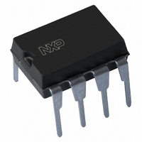
TEA1507P/N1,112 NXP Semiconductors, TEA1507P/N1,112 Datasheet - Page 5

TEA1507P/N1,112
Manufacturer Part Number
TEA1507P/N1,112
Description
IC CTRLR SMPS GREEN CM OVP 8DIP
Manufacturer
NXP Semiconductors
Series
GreenChip™ IIr
Datasheet
1.TEA1507PN1112.pdf
(20 pages)
Specifications of TEA1507P/N1,112
Package / Case
8-DIP (0.300", 7.62mm)
Output Isolation
Isolated
Frequency Range
6.5 ~ 175kHz
Voltage - Input
8.7 ~ 20 V
Voltage - Output
650V
Power (watts)
1W
Operating Temperature
-20°C ~ 145°C
Mounting Style
SMD/SMT
Lead Free Status / RoHS Status
Lead free / RoHS Compliant
Lead Free Status / RoHS Status
Lead free / RoHS Compliant, Lead free / RoHS Compliant
Other names
568-2336-5
935267356112
TEA1507PN
935267356112
TEA1507PN
Philips Semiconductors
PINNING
FUNCTIONAL DESCRIPTION
The TEA1507 is the controller of a compact flyback
converter, with the IC situated at the primary side. An
auxiliary winding of the transformer provides
demagnetization detection and powers the IC after
start-up.
The TEA1507 operates in multi modes.
The next converter stroke is started only after
demagnetization of the transformer current (zero current
switching), while the drain voltage has reached the lowest
voltage to prevent switching losses (green function). The
primary resonant circuit of primary inductance and drain
capacitor ensures this quasi-resonant operation. The
design can be optimized in such a way that zero voltage
switching can be reached over almost the universal mains
range.
To prevent very high frequency operation at lower loads,
the quasi-resonant operation changes smoothly in fixed
frequency PWM control.
At very low power (standby) levels, the frequency is
controlled down, via the VCO, to a minimum frequency of
about 6 kHz. Typically, 3 Watts can be achieved for a
75 W converter with an output power of 100 mW.
Start-up, mains enabling operation level and
undervoltage lock out (see Figs. 10 and 11)
Initially, the IC is self supplying from the rectified mains
voltage via pin DRAIN. Supply capacitor C
by the internal start-up current source to a level of about
4 V or higher, depending on the drain voltage. Once the
drain voltage exceeds the M-level (mains-dependent
operation-enabling level), the start-up current source will
2000 Dec 05
SYMBOL PIN
V
GND
CTRL
DEM
I
DRIVER
HVS
DRAIN
sense
CC
GreenChip II SMPS control IC
1
2
3
4
5
6
7
8
supply voltage
ground
control input
input from auxiliary winding for
demagnetization timing, OVP and OPP
programmable current sense input
gate driver output
high voltage safety spacer, not
connected
drain of external MOS switch, input for
start-up current and valley sensing
DESCRIPTION
VCC
is charged
5
continue charging capacitor C
opened), see Fig.2. The IC will activate the power
converter as soon as the voltage on pin V
V
winding as soon as the output voltage reaches its intended
level and the IC supply from the mains voltage is
subsequently stopped for high efficiency operation (green
function).
The moment the voltage on pin V
V
and enters a safe restart from the rectified mains voltage.
Inhibiting the auxiliary supply by external means causes
the converter to operate in a stable, well-defined burst
mode.
Supply management
All (internal) reference voltages are derived from a
temperature compensated, on-chip band gap circuit.
handbook, halfpage
handbook, halfpage
CC(start)
UVLO
(undervoltage lock out) level, the IC stops switching
level. The IC supply is taken over by the auxiliary
175 kHz
6 kHz
f
CTRL
Fig.4 Multi mode operation.
GND
DEM
V CC
VCO
Fig.3 Pin configuration.
1
2
3
4
TEA1507
fixed
MGU231
VCC
Preliminary specification
CC
(switch S1 will be
quasi resonant
8
7
6
5
drops below the
DRAIN
HVS
DRIVER
I sense
TEA1507
CC
passes the
MGU232
power


