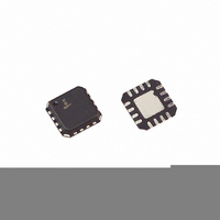
ISL6291-1CRZ Intersil, ISL6291-1CRZ Datasheet - Page 8

ISL6291-1CRZ
Manufacturer Part Number
ISL6291-1CRZ
Description
IC CHARGER LI-ION 4.1V 5X5 16QFN
Manufacturer
Intersil
Datasheet
1.ISL6291-1CRZ.pdf
(11 pages)
Specifications of ISL6291-1CRZ
Function
Charge Management
Battery Type
Lithium-Ion (Li-Ion), Lithium-Polymer (Li-Pol)
Voltage - Supply
4.35 V ~ 10 V
Operating Temperature
-20°C ~ 70°C
Mounting Type
Surface Mount
Package / Case
16-VQFN Exposed Pad, 16-HVQFN, 16-SQFN, 16-DHVQFN
Lead Free Status / RoHS Status
Lead free / RoHS Compliant
charge time exceeds the TIMEOUT interval, a fault is issued
and the charger is latched. The charger then enters the Fault
state.
The TIMEOUT limit is disabled when the TOEN pin is pulled
to LOW (see TOEN pin description for more information).
During the constant current charge mode, the STATUS pin
remains LOW and the FAULT pin remains HIGH.
Constant Voltage Charge Mode
The ISL6291 regulates the battery terminal voltage at V
the constant voltage mode. As the battery continues being
charged, the charge current starts to decrease, as shown in
Figure 1. When the charge current drops to the minimum
value I
completes. The total charge time for the constant current
mode and the constant voltage mode must not exceed the
TIMEOUT interval, unless the TOEN pin is pulled LOW;
otherwise, the charger also stops charging and indicates a
FAULT status. During the constant voltage mode, the
STATUS remains LOW and the FAULT remains HIGH.
Two versions of ISL6291 (see Ordering Information) are
available: a 4.1V termination voltage version, and a 4.2V
termination voltage version.
Inhibit State
The charger enters the Inhibit State once a normal charge
cycle completes. The ISL6291 then monitors the battery
voltage. Once the battery voltage falls below the V
threshold, a new charge cycle starts, as shown in Figure 1.
Both STATUS and FAULT are HIGH in this state.
Fault State
Two types of fault may occur during a charge cycle: the
TIMEOUT fault (refer to the TIME pin and the TOEN pin
description), and the temperature fault (see TEMP pin
description and the Battery Pack Temperature Monitoring
section). When a TIMEOUT fault occurs, the charger is
latched. The latch is released only by recycling the input
power or toggling the EN signal. When a temperature fault
occurs, the charger is reset and a new charge cycle starts
when the temperature fault ends. In case of a fault, the
FAULT pin indicates a logic LOW and the STATUS pin
outputs a logic HIGH.
Standby State
The charger is in the Standby State when the EN pin is held
LOW or the wall adapter is removed. The charger draws less
than 1
Timing Diagram
Figure 2 summarizes the operation of the charger and the
key signals after an adapter is attached to the charger input.
No fault occurs in this diagram and the EN pin is assumed
not connected to logic LOW.
µ
MIN
A of standby current when the adapter is removed.
, programmed by the IMIN pin, the charge cycle
8
RECHRG
CH
in
Internal Current Sensing
A 100,000:1 current mirror is employed to sense the current
in the pass element, as shown in the Block Diagram. The
current mirror is trimmed to 10% accuracy. The second
mirrored output, represented by I
is used to compare with the IMIN pin current to determine
the end-of-charge condition.
Charge Current Control
The charging current in the pass element is controlled by the
current amplifier CA, as shown in the Block Diagram. The
CA, the pass element, and the 100,000:1 current mirror form
a control loop. During a trickle charge mode or a constant
current charge mode, the control reference to the loop is the
reference current I
affect the loop operation because the battery voltage is lower
than the charge termination voltage V
amplifier output is blocked by the diode connecting to the
current reference. If the charge current in the PMOS pass
element is too high, its mirrored output is higher than the
reference I
has a higher voltage than the inverting input so that the
current amplifier output increases, reducing the gate-to-
source voltage of the PMOS pass element. The current in
the pass element thereby reduces. If the charge current is
too low, the current amplifier output reduces to force the
current to increase.
During the Trickle mode charge, the current reference
typically equals 1/10 of the current in the IREF pin. During
the constant current mode, the reference current equals the
current in the IREF pin.
If the temperature inside the IC rises above a typical value of
100°C, the current source block starts to reduce the reference
current I
temperature rise.
STATUS
I
CHARGE
FAULT
VBAT
V2P8
FIGURE 2. TIMING DIAGRAM AFTER AN ADAPTER IS
VIN
R
200us
POR
t
at a rate of 0.4µA/°C for every degree of
R
0
. The non-inverting input of the current amplifier
ATTACHED TO THE CHARGER INPUT
t
1
t
2
t
R
3
Charge Cycle
. The voltage amplifier VA does not
POR Threshold
1/8 TIMEOUT
15 Cycles to
3.0V V
t
4
MIN
V
RECHRG
SEN2
t
5
CH,
in the block diagram,
t
6
so that the voltage
t
7
Charge
15 Cycles
Cycle
May 2, 2005
t
8
FN9102.2


