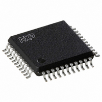
OM4068H/2,518 NXP Semiconductors, OM4068H/2,518 Datasheet - Page 14

OM4068H/2,518
Manufacturer Part Number
OM4068H/2,518
Description
IC LCD DRIVER 44-QFP
Manufacturer
NXP Semiconductors
Datasheet
1.OM4068H2518.pdf
(28 pages)
Specifications of OM4068H/2,518
Package / Case
44-MQFP, 44-PQFP
Display Type
LCD
Configuration
32 Segment
Interface
Serial
Current - Supply
12µA
Voltage - Supply
2.5 V ~ 5.5 V
Operating Temperature
-40°C ~ 105°C
Mounting Type
Surface Mount
Number Of Digits
12
Number Of Segments
96
Maximum Clock Frequency
2.1 MHz
Operating Supply Voltage
2.5 V to 5.5 V
Maximum Power Dissipation
500 mW
Maximum Operating Temperature
+ 105 C
Attached Touch Screen
No
Maximum Supply Current
25 uA
Minimum Operating Temperature
- 40 C
Lead Free Status / RoHS Status
Lead free / RoHS Compliant
Digits Or Characters
-
Lead Free Status / Rohs Status
Lead free / RoHS Compliant
Other names
568-4513-2
935276329518
OM4068HB-T
OM4068HB-T
935276329518
OM4068HB-T
OM4068HB-T
Available stocks
Company
Part Number
Manufacturer
Quantity
Price
Company:
Part Number:
OM4068H/2,518
Manufacturer:
NXP Semiconductors
Quantity:
10 000
Philips Semiconductors
Display latch
The 96-bit display latch holds the display data while the
corresponding multiplex signals are generated. There is a
one-to-one relationship between the data in the display
latch and the LCD segment outputs. An LCD segment is
activated when the corresponding data bit in the display
latch is HIGH.
Display latches are in HOLD mode (SCE HIGH) during the
shift operation to maintain the display data constant.
Data are latched into the display latch with the internal
frame clock. Thus there is a delay of up to one half frame
before new data are latched after signal SCE returns to
zero.
Shift register configuration
1998 Jun 18
handbook, full pagewidth
LCD driver for low multiplex rates
SDIN
SDIN
SDIN
D1A
D1A
D1A
1
32-bit register
32-bit register
32-bit register
Fig.9 Display data bit position in shift register.
driving mode: duplex (1 : 2); (M1, M0) = 10
driving mode: triplex (1 : 3); (M1, M0) = 11
driving mode: static; (M1, M0) = 01
96-bit shift register
D32A
D32A
D32A
32
D1B
D1B
SDOUT
32-bit register
32-bit register
14
Timing
The timing of the OM4068 organizes the internal data flow
of the device. This includes the transfer of display data
from the shift register to the display segments outputs.
The timing also generates the LCD frame frequency which
is derived from the clock frequency generated in the
internal clock generator:
f
fr(LCD)
D32B
D32B
64
=
D1C
------------ -
2400
f
SDOUT
osc
32-bit register
D32C
96
SDOUT
MBK823
Product specification
OM4068


