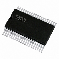
PCF8566T/1,118 NXP Semiconductors, PCF8566T/1,118 Datasheet - Page 19

PCF8566T/1,118
Manufacturer Part Number
PCF8566T/1,118
Description
IC LCD DVR UNVRSL LOW-MUX 40VSOP
Manufacturer
NXP Semiconductors
Datasheet
1.PCF8566T1118.pdf
(48 pages)
Specifications of PCF8566T/1,118
Package / Case
40-VSOP
Display Type
LCD
Configuration
7 Segment + DP, 14 Segment (24 Segment)
Interface
I²C
Current - Supply
30µA
Voltage - Supply
2.5 V ~ 6 V
Operating Temperature
-40°C ~ 85°C
Mounting Type
Surface Mount
Number Of Digits
12
Number Of Segments
96
Maximum Clock Frequency
315 KHz
Operating Supply Voltage
2.5 V to 6 V
Maximum Power Dissipation
400 mW
Maximum Operating Temperature
+ 85 C
Maximum Supply Current
90 uA
Minimum Operating Temperature
- 40 C
Lead Free Status / RoHS Status
Lead free / RoHS Compliant
Digits Or Characters
-
Lead Free Status / Rohs Status
Lead free / RoHS Compliant
Other names
568-1070-2
935278688118
PCF8566TD-T
935278688118
PCF8566TD-T
NXP Semiconductors
PCF8566_7
Product data sheet
7.13 Sub-address counter
7.14 Output bank selector
7.15 Input bank selector
7.16 Blinker
The storage of display data is conditioned by the contents of the subaddress counter.
Storage is allowed to take place only when the contents of the subaddress counter match
with the hardware subaddress applied to A0, A1 and A2. The subaddress counter value is
defined by the device select command (see
subaddress counter and the hardware subaddress do not match then data storage is
blocked but the data pointer will be incremented as if data storage had taken place. The
subaddress counter is also incremented when the data pointer overflows.
The storage arrangements described lead to extremely efficient data loading in cascaded
applications. When a series of display bytes are sent to the display RAM, automatic
wrap-over to the next PCF8566 occurs when the last RAM address is exceeded.
Subaddressing across device boundaries is successful even if the change to the next
device in the cascade occurs within a transmitted character (such as during the 14th
display data byte transmitted in 1:3 multiplex mode).
The output bank selector (see
address for transfer to the display register. The actual bit selected depends on the LCD
drive mode in operation and on the instant in the multiplex sequence.
The PCF8566 includes a RAM bank switching feature in the static and 1:2 multiplex drive
modes. In the static drive mode, the bank select command may request the contents of
bit 2 to be selected for display instead of the contents of bit 0. In 1:2 multiplex drive mode,
the contents of bits 2 and 3 may be selected instead of bits 0 and 1. This enables
preparation of display information in an alternative bank and the ability to switch to it once
it has been assembled.
The input bank selector loads display data into the display RAM based on the selected
LCD drive configuration. Using the bank select command, display data can be loaded in
bit 2 into static drive mode or in bits 2 and 3 into 1:2 multiplex drive mode. The input bank
selector functions independently of the output bank selector.
The display blinking capabilities of the PCF8566 are very versatile. The whole display can
be blinked at frequencies selected by the blink command. The blinking frequencies are
integer fractions of the clock frequency; the ratios between the clock and blinking
frequencies depend on the mode in which the device is operating (see
•
•
•
•
In 1:4 multiplex mode: all RAM addresses of bit 0 are selected, followed sequentially
by the contents of bit 1, bit 2 and then bit 3.
In 1:3 multiplex mode: bits 0, 1 and 2 are selected sequentially.
In 1:2 multiplex mode: bits 0 and 1 are selected.
In the static mode: bit 0 is selected.
Rev. 07 — 25 February 2009
Table
15), selects one of the four bits per display RAM
Universal LCD driver for low multiplex rates
Table 14
and
Table
21). If the contents of the
PCF8566
Table
© NXP B.V. 2009. All rights reserved.
7).
19 of 48


