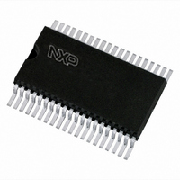
PCF8566T/1,118 NXP Semiconductors, PCF8566T/1,118 Datasheet - Page 27

PCF8566T/1,118
Manufacturer Part Number
PCF8566T/1,118
Description
IC LCD DVR UNVRSL LOW-MUX 40VSOP
Manufacturer
NXP Semiconductors
Datasheet
1.PCF8566T1118.pdf
(48 pages)
Specifications of PCF8566T/1,118
Package / Case
40-VSOP
Display Type
LCD
Configuration
7 Segment + DP, 14 Segment (24 Segment)
Interface
I²C
Current - Supply
30µA
Voltage - Supply
2.5 V ~ 6 V
Operating Temperature
-40°C ~ 85°C
Mounting Type
Surface Mount
Number Of Digits
12
Number Of Segments
96
Maximum Clock Frequency
315 KHz
Operating Supply Voltage
2.5 V to 6 V
Maximum Power Dissipation
400 mW
Maximum Operating Temperature
+ 85 C
Maximum Supply Current
90 uA
Minimum Operating Temperature
- 40 C
Lead Free Status / RoHS Status
Lead free / RoHS Compliant
Digits Or Characters
-
Lead Free Status / Rohs Status
Lead free / RoHS Compliant
Other names
568-1070-2
935278688118
PCF8566TD-T
935278688118
PCF8566TD-T
NXP Semiconductors
10. Limiting values
PCF8566_7
Product data sheet
CAUTION
Table 18.
In accordance with the Absolute Maximum Rating System (IEC 60134).
[1]
[2]
[3]
[4]
[5]
Symbol
V
V
V
V
I
I
I
I
I
P
P
T
V
I
I
O
DD
SS
DD(LCD)
lu
stg
DD
LCD
I
O
tot
o
esd
Values with respect to V
According to the NXP store and transport conditions (document SNW-SQ-623 ) the devices have to be
stored at a temperature of +5 C to +45 C and a humidity of 25 % to 75 %.
Pass level; Human Body Model (HBM) according to JESD22-A114.
Pass level; Machine Model (MM), according to JESD22-A115.
Pass level; latch-up testing, according to JESD78.
Static voltages across the liquid crystal display can build up when the LCD supply voltage
(V
display artifacts. To avoid such artifacts, V
LCD
) is on while the IC supply voltage (V
Limiting values
Parameter
supply voltage
LCD supply voltage
input voltage
output voltage
input current
output current
supply current
ground supply
current
LCD supply current
total power
dissipation
output power
storage
temperature
electrostatic
discharge voltage
latch-up current
Rev. 07 — 25 February 2009
DD
.
Conditions
on each of the pins SCL,
SDA, A0 to A2, OSC, CLK,
SYNC and SA0
on each of the pins S0 to S23
and BP0 to BP3
per package
HBM
MM
Universal LCD driver for low multiplex rates
LCD
DD
) is off, or vice versa. This may cause unwanted
and V
DD
must be applied or removed together.
[1]
[1]
[2]
[3]
[4]
[5]
Min
-
-
-
-
-
0.5
0.5
0.5
0.5
20
25
50
50
50
65
PCF8566
© NXP B.V. 2009. All rights reserved.
Max
7.0
7.0
7.0
7.0
+20
+25
+50
+50
+50
400
100
+150
100
2000
200
Unit
V
V
V
V
mA
mA
mA
mA
mA
mW
mW
V
V
mA
C
27 of 48


