PCA8534AH/Q900/1,5 NXP Semiconductors, PCA8534AH/Q900/1,5 Datasheet
PCA8534AH/Q900/1,5
Specifications of PCA8534AH/Q900/1,5
Available stocks


Related parts for PCA8534AH/Q900/1,5


PCA8534AH/Q900/1,5 Summary of contents
Page 1
PCA8534A Universal LCD driver for low multiplex rates Rev. 02 — 1 June 2010 1. General description The PCA8534A is a peripheral device which interfaces to almost any Liquid Crystal Display (LCD) multiplexed LCD containing up to four backplanes and ...
Page 2
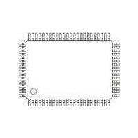
... NXP Semiconductors 3. Ordering information Table 1. Type number PCA8534AH/Q900 LQFP80 plastic low profile quad flat package; 4. Marking Table 2. Type number PCA8534AH/Q900 PCA8534A_2 Product data sheet Ordering information Package Name Description 80 leads; body 12 × 12 × 1.4 mm Marking codes All information provided in this document is subject to legal disclaimers. ...
Page 3
... NXP Semiconductors 5. Block diagram V LCD LCD BIAS GENERATOR V SS CLK CLOCK SELECT AND TIMING SYNC OSC OSCILLATOR SCL INPUT FILTERS SDA Fig 1. Block diagram of PCA8534A PCA8534A_2 Product data sheet BP0 BP1 BP2 BP3 BACKPLANE OUTPUTS LCD VOLTAGE SELECTOR DISPLAY CONTROL PCA8534A ...
Page 4
... NXP Semiconductors 6. Pinning information 6.1 Pinning S31 S32 S33 S34 S35 S36 S37 S38 S39 S40 S41 S42 S43 S44 S45 S46 S47 S48 S49 S50 Fig 2. PCA8534A_2 Product data sheet PCA8534AH Top view. For mechanical details, see Pin configuration for LQFP80 (PCA8534AH) All information provided in this document is subject to legal disclaimers. Rev. 02 — ...
Page 5
... NXP Semiconductors 6.2 Pin description Table 3. Symbol S31 to S59 BP0 to BP3 n.c. SDA SCL CLK V DD SYNC OSC SA0 LCD S0 to S30 PCA8534A_2 Product data sheet Pin description Pin Type Description output LCD segment output output LCD backplane output not connected; do not connect and do not use as feed ...
Page 6
... NXP Semiconductors 7. Functional description The PCA8534A is a versatile peripheral device designed to interface any microprocessor or microcontroller to a wide variety of LCDs. It can directly drive any static or multiplexed LCD containing up to four backplanes and segments. The possible display configurations of the PCA8534A depend on the number of active backplane outputs required ...
Page 7
... NXP Semiconductors • The data pointer and the subaddress counter are cleared (set to logic 0) • The display is disabled Remark: Do not transfer data on the I the reset action to complete. 7.2 LCD bias generator Fractional LCD biasing voltages are obtained from an internal voltage divider of three ...
Page 8
... NXP Semiconductors for 1:3 multiplex drive mode for 1:4 multiplex drive mode The RMS off-state voltage ( off RMS Discrimination is the ratio ---------------------- - off RMS Using Equation ⁄ 1 bias is 2 ⁄ 1 bias is 2 The advantage of these LCD drive modes is a reduction of the LCD full scale voltage V as follows: • ...
Page 9
... NXP Semiconductors 7.4 LCD drive mode waveforms 7.4.1 Static drive mode The static LCD drive mode is used when a single backplane is provided in the LCD. Backplane and segment drive waveforms for this mode are shown in Fig 4. PCA8534A_2 Product data sheet V LCD BP0 V SS ...
Page 10
... NXP Semiconductors 7.4.2 1:2 Multiplex drive mode When two backplanes are provided in the LCD, the 1:2 multiplex mode applies. The PCA8534A allows the use of Figure 6. Fig 5. PCA8534A_2 Product data sheet ⁄ 1 bias LCD BP0 LCD LCD BP1 LCD LCD LCD Sn+1 ...
Page 11
... NXP Semiconductors Fig 6. PCA8534A_2 Product data sheet V LCD LCD BP0 LCD LCD LCD BP1 LCD LCD LCD LCD LCD LCD S n LCD LCD LCD LCD state − LCD − LCD −V LCD V LCD LCD LCD 0 V state 2 − LCD − LCD − ...
Page 12
... NXP Semiconductors 7.4.3 1:3 Multiplex drive mode When three backplanes are provided in the LCD, the 1:3 multiplex drive mode applies, as shown in Fig 7. PCA8534A_2 Product data sheet Figure 7. V LCD LCD BP0 LCD LCD LCD BP1 LCD LCD LCD BP2 LCD V SS ...
Page 13
... NXP Semiconductors 7.4.4 1:4 Multiplex drive mode When four backplanes are provided in the LCD, the 1:4 multiplex drive mode applies, as shown in BP0 BP1 BP2 BP3 Sn Sn+1 Sn+2 Sn+3 state 1 state 2 Fig 8. PCA8534A_2 Product data sheet Figure 8. V LCD LCD LCD V SS ...
Page 14
... NXP Semiconductors 7.5 Oscillator The internal logic and the LCD drive signals of the PCA8534A are timed by the frequency f , which equals either the built-in oscillator frequency f clk f . The clock frequency f clk(ext) 7.5.1 Internal clock The internal oscillator is enabled by connecting pin OSC to pin V output from pin CLK is the clock signal for any cascaded PCA8534A in the system ...
Page 15
... NXP Semiconductors If less than four backplane outputs are required the unused outputs can be left as an open-circuit. • In 1:3 multiplex drive mode: BP3 carries the same signal as BP1, therefore these two adjacent outputs can be tied together to give enhanced drive capabilities. • In 1:2 multiplex drive mode: BP0 and BP2, BP1 and BP3 respectively carry the same signals and can also be paired to increase the drive capabilities. • ...
Page 16
LCD segments LCD backplanes S a n+2 BP0 n+3 n+1 static n+5 n n+6 BP0 1 ...
Page 17
... NXP Semiconductors The following applies to • Static mode: the eight transmitted data bits are placed in row 0 to eight successive display RAM addresses. • 1:2 multiplex mode: the eight transmitted data bits are placed in row 0 and 1 to four successive display RAM addresses. ...
Page 18
... NXP Semiconductors This last step is very important because during writing data to the first PCA8534A, the data pointer of the second PCA8534A is incremented. In addition, the hardware subaddress should not be changed whilst the device is being accessed on the I interface. 7.13 Output bank selector The output bank selector (see address for transfer to the display register ...
Page 19
... NXP Semiconductors Table 7. Assuming that f Blink mode Off additional feature is for the arbitrary selection of LCD segments to be blinked. This applies to the static and 1:2 multiplex drive modes and is implemented without any communication overheads. Using the output bank selector, the displayed RAM banks are exchanged with alternate RAM banks at the blinking frequency ...
Page 20
... NXP Semiconductors 7.16.2 START and STOP conditions Both data and clock lines remain HIGH when the bus is not busy. A HIGH-to-LOW transition of the data line while the clock is HIGH is defined as the START condition - S. A LOW-to-HIGH transition of the data line while the clock is HIGH is defined as the STOP ...
Page 21
... NXP Semiconductors • A master receiver must signal an end of data to the transmitter by not generating an acknowledge on the last byte that has been clocked out of the slave. In this event, the transmitter must leave the data line HIGH to enable the master to generate a STOP condition. Acknowledgement on the I Fig 14 ...
Page 22
... NXP Semiconductors The PCA8534A is a write-only device and will not respond to a read access, therefore bit 0 should always be logic 0. Bit 1 of the slave address byte that a PCA8534A will respond to, is defined by the level tied to its SA0 input (V Having two reserved slave addresses allows the following on the same I • ...
Page 23
... NXP Semiconductors Table 9. Bit The command bytes and control bytes are also acknowledged by all addressed PCA8534A connected to the bus. The display bytes are stored in the display RAM at the address specified by the data pointer and the subaddress counter. Both data pointer and subaddress counter are automatically updated ...
Page 24
... NXP Semiconductors Table 11. Bit Table 12. Bit Table 13. Bit Table 14. Bit [1] The bank select command has no effect in 1:3 or 1:4 multiplex drive modes. PCA8534A_2 Product data sheet Mode-set command bit description Symbol Value Description - 1100 fixed value E display status the possibility to disable the display allows implementation of ...
Page 25
... NXP Semiconductors Table 15. Bit [1] Only normal blinking can be selected in multiplexer 1:3 or 1:4 drive modes. [2] The blink frequencies are shown in 7.18 Display controller The display controller executes the commands identified by the command decoder. It contains the status registers of the PCA8534A and coordinates their effects. ...
Page 26
... NXP Semiconductors 8. Internal circuitry Fig 17. Device protection diagram PCA8534A_2 Product data sheet Universal LCD driver for low multiplex rates V DD SA0 CLK OSC SYNC A0, A1 LCD BP0, BP1, BP2, BP3 LCD S0 to S59 V SS All information provided in this document is subject to legal disclaimers. ...
Page 27
... NXP Semiconductors 9. Limiting values CAUTION Static voltages across the liquid crystal display can build up when the LCD supply voltage (V LCD display artifacts. To avoid such artifacts, V Table 16. In accordance with the Absolute Maximum Rating System (IEC 60134). Symbol LCD I DD(LCD tot P/out ...
Page 28
... NXP Semiconductors 10. Static characteristics Table 17. Static characteristics Symbol Parameter Supplies V supply voltage DD V LCD supply voltage LCD I supply current DD I LCD supply current DD(LCD) Logic V input voltage I V LOW-level input voltage IL V HIGH-level input voltage IH V power-on reset voltage POR I LOW-level output current output sink current ...
Page 29
... NXP Semiconductors Fig 18. Typical I Fig 19. Typical I PCA8534A_2 Product data sheet (μ °C; 1:4 multiplex 6 amb LCD 2 display connected; I C-bus inactive. with respect DD(LCD) (μ °C; 1:4 multiplex 1.536 kHz; all RAM written with logic 1; no display connected. amb clk(ext) with respect to V DD(LCD) All information provided in this document is subject to legal disclaimers ...
Page 30
... NXP Semiconductors 11. Dynamic characteristics Table 18. Dynamic characteristics Symbol Parameter Clock Internal: output pin CLK f oscillator frequency osc External: input pin CLK f external clock frequency clk(ext) t HIGH-level clock time clk(H) t LOW-level clock time clk(L) Synchronization: input pin SYNC t SYNC propagation delay ...
Page 31
... NXP Semiconductors BP0 to BP3, and S0 to S59 Fig 20. Driver timing waveforms SDA SCL SDA Fig 21. I PCA8534A_2 Product data sheet clk t clk(H) CLK SYNC t PD(SYNC_N BUF LOW t HD;STA 2 C-bus timing waveforms All information provided in this document is subject to legal disclaimers. Rev. 02 — 1 June 2010 ...
Page 32
... NXP Semiconductors 12. Application information 12.1 Cascaded operation Large display configurations PCA8534A can be recognized on the same 2 I C-bus by using the 3-bit hardware subaddress (A0, A1, and A2) and the programmable 2 I C-bus slave address (SA0). Table 19. Cluster cascaded PCA8534A are synchronized, they can share the backplane signals from one of the devices in the cascade ...
Page 33
... NXP Semiconductors V LCD V DD PROCESSOR/ CONTROLLER V SS Fig 22. Cascaded PCA8534A configuration The SYNC line is provided to maintain the correct synchronization between all cascaded PCA8534A. Synchronization is guaranteed after a power-on reset. The only time that SYNC is likely to be needed is if synchronization is accidentally lost (e.g. by noise in adverse electrical environments or by defining a multiplex mode when PCA8534A with different SA0 levels are cascaded) ...
Page 34
... NXP Semiconductors Fig 23. Synchronization of the cascade for various PCA8534A drive modes The contact resistance between the SYNC pins of cascaded devices must be controlled. If the resistance is too high, the device will not be able to synchronize properly. Table 20 Table 20. Number of devices The PCA8534A can always be cascaded with other devices of the same type or conditionally with other devices of the same family ...
Page 35
... NXP Semiconductors In a cascaded configuration only one PCA8534A master must be used as clock source. All other PCA8534A in the cascade must be configured as slave such that they receive the clock from the master external clock source is used, all PCA8534A in the cascade must be configured such ...
Page 36
... NXP Semiconductors 13. Package outline LQFP80: plastic low profile quad flat package; 80 leads; body 1 pin 1 index DIMENSIONS (mm are the original dimensions) A UNIT max. 0.16 1.5 1.6 mm 0.25 0.04 1.3 Note 1. Plastic or metal protrusions of 0.25 mm maximum per side are not included. OUTLINE VERSION ...
Page 37
... NXP Semiconductors 14. Handling information All input and output pins are protected against ElectroStatic Discharge (ESD) under normal handling. When handling Metal-Oxide Semiconductor (MOS) devices ensure that all normal precautions are taken as described in JESD625-A, IEC 61340-5 or equivalent standards. 15. Soldering of SMD packages This text provides a very brief insight into a complex technology. A more in-depth account of soldering ICs can be found in Application Note AN10365 “ ...
Page 38
... NXP Semiconductors 15.3 Wave soldering Key characteristics in wave soldering are: • Process issues, such as application of adhesive and flux, clinching of leads, board transport, the solder wave parameters, and the time during which components are exposed to the wave • Solder bath specifications, including temperature and impurities 15 ...
Page 39
... NXP Semiconductors Fig 25. Temperature profiles for large and small components For further information on temperature profiles, refer to Application Note AN10365 “Surface mount reflow soldering description”. PCA8534A_2 Product data sheet maximum peak temperature = MSL limit, damage level temperature minimum peak temperature = minimum soldering temperature MSL: Moisture Sensitivity Level All information provided in this document is subject to legal disclaimers ...
Page 40
... NXP Semiconductors 16. Abbreviations Table 23. Acronym AEC CMOS CDM DC HBM LCD LSB MM MSB MSL PCB POR RAM RC RMS SCL SDA SMD PCA8534A_2 Product data sheet Abbreviations Description Automotive Electronics Council Complementary Metal-Oxide Semiconductor Charged Device Model Direct Current Human Body Model Inter-Integrated Circuit ...
Page 41
... NXP Semiconductors 17. References [1] AN10365 — Surface mount reflow soldering description [2] IEC 60134 — Rating systems for electronic tubes and valves and analogous semiconductor devices [3] IEC 61340-5 — Protection of electronic devices from electrostatic phenomena [4] IPC/JEDEC J-STD-020D — Moisture/Reflow Sensitivity Classification for Nonhermetic Solid State Surface Mount Devices [5] JESD22-A114 — ...
Page 42
... In no event shall NXP Semiconductors be liable for any indirect, incidental, punitive, special or consequential damages (including - without limitation - lost profits, lost savings, business interruption, costs related to the removal or ...
Page 43
... NXP Semiconductors Export control — This document as well as the item(s) described herein may be subject to export control regulations. Export might require a prior authorization from national authorities. 20. Contact information For more information, please visit: For sales office addresses, please send an email to: PCA8534A_2 Product data sheet 19 ...
Page 44
... NXP Semiconductors 21. Contents 1 General description . . . . . . . . . . . . . . . . . . . . . . 1 2 Features and benefits . . . . . . . . . . . . . . . . . . . . 1 3 Ordering information . . . . . . . . . . . . . . . . . . . . . 2 4 Marking . . . . . . . . . . . . . . . . . . . . . . . . . . . . . . . . 2 5 Block diagram . . . . . . . . . . . . . . . . . . . . . . . . . . 3 6 Pinning information . . . . . . . . . . . . . . . . . . . . . . 4 6.1 Pinning . . . . . . . . . . . . . . . . . . . . . . . . . . . . . . . 4 6.2 Pin description . . . . . . . . . . . . . . . . . . . . . . . . . 5 7 Functional description . . . . . . . . . . . . . . . . . . . 6 7.1 Power-On Reset (POR 7.2 LCD bias generator . . . . . . . . . . . . . . . . . . . . . 7 7.3 LCD voltage selector . . . . . . . . . . . . . . . . . . . . 7 7.4 LCD drive mode waveforms ...