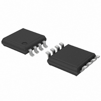
PCA9511ADP,118 NXP Semiconductors, PCA9511ADP,118 Datasheet - Page 7

PCA9511ADP,118
Manufacturer Part Number
PCA9511ADP,118
Description
IC HOTSWAP I2C/SMBUS BUFF 8TSSOP
Manufacturer
NXP Semiconductors
Type
I²C-Bus and SMBus Switchr
Datasheet
1.PCA9511ADP118.pdf
(24 pages)
Specifications of PCA9511ADP,118
Package / Case
8-TSSOP
Applications
Hot-Swap/SMB Buffer
Internal Switch(s)
Yes
Current Limit
50mA
Voltage - Supply
2.7 V ~ 5.5 V
Operating Temperature
-40°C ~ 85°C
Mounting Type
Surface Mount
Logic Family
PCA
Maximum Operating Temperature
85 C
Mounting Style
SMD/SMT
Minimum Operating Temperature
- 40 C
Number Of Lines (input / Output)
3 / 3
Propagation Delay Time
70 ns
Logic Type
Bus Buffer
Lead Free Status / RoHS Status
Lead free / RoHS Compliant
Lead Free Status / RoHS Status
Lead free / RoHS Compliant, Lead free / RoHS Compliant
Other names
568-3360-2
935279308118
PCA9511ADP-T
935279308118
PCA9511ADP-T
Available stocks
Company
Part Number
Manufacturer
Quantity
Price
Part Number:
PCA9511ADP,118
Manufacturer:
NXP/恩智浦
Quantity:
20 000
NXP Semiconductors
PCA9511A_4
Product data sheet
8.5 Rise time accelerators
8.6 READY digital output
8.7 ENABLE low current disable
8.8 Resistor pull-up value selection
turn-on delay and the falling edge slew rate. The output falling edge slew rate is a function
of the internal maximum slew rate which is a function of temperature, V
well as the load current and the load capacitance.
During positive bus transitions a 2 mA current source is switched on to quickly slew the
SDA and SCL lines HIGH once the input level of 0.6 V for the PCA9511A is exceeded.
The rising edge rate should be at least 1.25 V/ s to guarantee turn on of the accelerators.
The built-in V t rise time accelerators on all SDA and SCL lines requires the bus pull-up
voltage and supply voltage (V
This pin provides a digital flag which is LOW when either ENABLE is LOW or the start-up
sequence described earlier in this section has not been completed. READY goes HIGH
when ENABLE is HIGH and start-up is complete. The pin is driven by an open-drain
pull-down capable of sinking 3 mA while holding 0.4 V on the pin. Connect a resistor of
10 k to V
Grounding the ENABLE pin disconnects the backplane side from the card side, disables
the rise time accelerators, drives READY LOW, disables the bus precharge circuitry, and
puts the part in a low current state. When the pin voltage is driven all the way to V
part waits for data transactions on both the backplane and card sides to be complete
before reconnecting the two sides.
The system pull-up resistors must be strong enough to provide a positive slew rate of
1.25 V/ s on the SDA and SCL pins, in order to activate the boost pull-up currents during
rising edges. Choose maximum resistor value using the formula given in
where R is the pull-up resistor value in , V
and C is the equivalent bus capacitance in picofarads (pF).
In addition, regardless of the bus capacitance, always choose R
maximum, R
voltages on SDAOUT and SCLOUT to connect the backplane to the card, and these
pull-up values are needed to overcome the precharge voltage. See the curves in
and
R 800 10
Figure 6
CC
3
for guidance in resistor pull-up selection.
to provide the pull-up.
V
---------------------------------- -
45 k for V
CC min
C
Rev. 04 — 19 August 2009
–
0.6
CC
= 3.6 V maximum. The start-up circuitry requires logic HIGH
CC
) to be the same.
Hot swappable I
CC(min)
is the minimum V
2
C-bus and SMBus bus buffer
65.7 k for V
PCA9511A
CC
CC
voltage in volts,
© NXP B.V. 2009. All rights reserved.
Equation
and process, as
CC
Figure 5
CC
= 5.5 V
1:
7 of 24
, the
(1)


