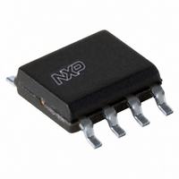
PCA9514AD,112 NXP Semiconductors, PCA9514AD,112 Datasheet - Page 16

PCA9514AD,112
Manufacturer Part Number
PCA9514AD,112
Description
IC I2C/SMBUS BUFF 8-SOIC
Manufacturer
NXP Semiconductors
Type
I²C-Bus and SMBus Switchr
Datasheet
1.PCA9514ADP118.pdf
(26 pages)
Specifications of PCA9514AD,112
Package / Case
8-SOIC (0.154", 3.90mm Width)
Applications
Hot-Swap/SMB Buffer
Internal Switch(s)
Yes
Current Limit
50mA
Voltage - Supply
2.7 V ~ 5.5 V
Operating Temperature
-40°C ~ 85°C
Mounting Type
Surface Mount
Logic Family
PCA
Supply Voltage (max)
7 V
Supply Voltage (min)
- 0.5 V
Maximum Operating Temperature
+ 85 C
Mounting Style
SMD/SMT
Minimum Operating Temperature
- 40 C
Output Voltage
0.3 V
Propagation Delay Time
80 ns
Supply Current
3.5 mA
Logic Type
SMBus Bus Buffer
Operating Temperature (min)
-40C
Operating Temperature Classification
Industrial
Operating Temperature (max)
85C
Package Type
SO
Rad Hardened
No
Lead Free Status / RoHS Status
Lead free / RoHS Compliant
Lead Free Status / RoHS Status
Lead free / RoHS Compliant, Lead free / RoHS Compliant
Other names
568-3365-5
935279867112
PCA9514AD
935279867112
PCA9514AD
NXP Semiconductors
[3]
[4]
[5]
[6]
[7]
[8]
[9]
PCA9513A_PCA9514A_4
Product data sheet
Fig 14. I
Fig 16. Input/output t
Delays that can occur after ENABLE and/or idle times have passed.
Guaranteed by design, not production tested.
I
Input pull-up voltage should not exceed power supply voltage in operating mode because the rise time accelerator will clamp the voltage
to the positive supply rail.
The connection circuitry always regulates its output to a higher voltage than its input. The magnitude of this offset voltage as a function
of the pull-up resistor and V
C
Force V
output.
trt(pu)
(mA)
t
(ns)
I
PHL
b
CC
= total capacitance of one bus line in pF.
3.7
3.3
2.9
2.5
90
80
70
60
varies with temperature and V
40
40
C
CC
SDAIN
i
= C
versus temperature
o
= V
11.1 Typical performance characteristics
> 100 pF; R
SCLIN
V
CC
= 0.1 V, tie SDAOUT and SCLOUT through 10 k resistor to V
= 5.5 V
PHL
2.7 V
3.3 V
PU(in)
CC
versus temperature
+25
+25
voltage is shown in
= R
PU(out)
CC
V
T
T
CC
amb
amb
voltage, as shown in
= 5.5 V
3.3 V
2.7 V
= 10 k
( C)
( C)
002aab588
002aab589
Section 11.1 “Typical performance
+90
+90
Rev. 04 — 18 August 2009
Section 11.1 “Typical performance
Fig 15. I
Fig 17. Connection circuitry V
V
I
(mA)
trt(pu)
(mV)
O
350
250
150
Hot swappable I
12
50
PCA9513A; PCA9514A
V
8
4
0
I
40
0
trt(pu)
versus temperature
CC
characteristics”.
10
and measure the SDAOUT and SCLOUT
characteristics”.
2
C-bus and SMBus bus buffer
+25
20
V
CC
O
= 5 V
3.3 V
T
V
amb
V
CC
I
30
= 5 V
© NXP B.V. 2009. All rights reserved.
3.0 V
2.7 V
( C)
R
002aab590
002aab591
PU
(k )
+90
40
16 of 26


