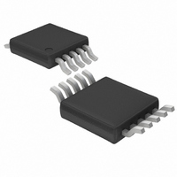
LTC4252A-2IMS Linear Technology, LTC4252A-2IMS Datasheet - Page 18

LTC4252A-2IMS
Manufacturer Part Number
LTC4252A-2IMS
Description
IC CTRLR HOTSWAP NEG VOLT 10MSOP
Manufacturer
Linear Technology
Type
Hot-Swap Controllerr
Specifications of LTC4252A-2IMS
Applications
General Purpose
Internal Switch(s)
No
Operating Temperature
-40°C ~ 85°C
Mounting Type
Surface Mount
Package / Case
10-TFSOP, 10-MSOP (0.118", 3.00mm Width)
Family Name
LTC4252A-2
Package Type
MSOP
Operating Temperature (min)
-40C
Operating Temperature (max)
85C
Operating Temperature Classification
Industrial
Product Depth (mm)
3mm
Product Height (mm)
0.86mm
Product Length (mm)
3mm
Mounting
Surface Mount
Pin Count
10
Lead Free Status / RoHS Status
Contains lead / RoHS non-compliant
Lead Free Status / RoHS Status
Contains lead / RoHS non-compliant
Available stocks
Company
Part Number
Manufacturer
Quantity
Price
Company:
Part Number:
LTC4252A-2IMS
Manufacturer:
LT
Quantity:
10 000
Part Number:
LTC4252A-2IMS
Manufacturer:
LINEAR/凌特
Quantity:
20 000
Part Number:
LTC4252A-2IMS#TRPBF
Manufacturer:
LT/凌特
Quantity:
20 000
LTC4252-1/LTC4252-2
LTC4252A-1/LTC4252A-2
APPLICATIONS INFORMATION
and eliminates current spikes at insertion. A large external
gate-source capacitor is thus unnecessary for the purpose
of compensating C
capacitor C
for the analog current limit loop.
GATE has two comparators: the GATE low comparator
looks for < 0.5V threshold prior to initial timing or a GATE
start-up cycle; the GATE high comparator looks for < 2.8V
relative to V
tor, sets PWRGD status during GATE startup.
SENSE
The SENSE pin is monitored by the circuit breaker (CB)
comparator, the analog current limit (ACL) amplifier and
the fast current limit (FCL) comparator. Each of these three
measures the potential of SENSE relative to V
SENSE exceeds 50mV, the CB comparator activates the
230μA TIMER pull-up. At 100mV (60mV for the LTC4252A),
the ACL amplifier servos the MOSFET current and, at
200mV, the FCL comparator abruptly pulls GATE low in
an attempt to bring the MOSFET current under control. If
any of these conditions persists long enough for TIMER
to charge C
down and pulls GATE low.
If the SENSE pin encounters a voltage greater than V
the ACL amplifier will servo GATE downwards in an attempt
to control the MOSFET current. Since GATE overdrives the
MOSFET in normal operation, the ACL amplifier needs time
to discharge GATE to the threshold of the MOSFET. For a
mild overload the ACL amplifier can control the MOSFET
current, but in the event of a severe overload the current
may overshoot. At SENSE = 200mV the FCL comparator
takes over, quickly discharging the GATE pin to near V
potential. FCL then releases and the ACL amplifier takes
over. All the while TIMER is running. The effect of FCL is
to add a nonlinear response to the control loop in favor
of reducing MOSFET current.
Owing to inductive effects in the system, FCL typically
overcorrects the current limit loop and GATE undershoots.
A zero in the loop (resistor R
pacitor) helps the ACL amplifier to recover.
18
C
IN
T
is adequate. C
to 4V (see Equation 3), the LTC4252 shuts
and, together with the DRAIN low compara-
GD
. Instead, a smaller value (≥ 10nF)
C
also provides compensation
C
in series with the gate ca-
EE
. When
ACL
EE
,
SHORT-CIRCUIT OPERATION
Circuit behavior arising from a load side low impedance
short is shown in Figure 6 for the LTC4252. Initially, the
current overshoots the fast current limit level of V
200mV (Trace 2) as the GATE pin works to bring V
control (Trace 3). The overshoot glitches the backplane
in the negative direction and when the current is reduced
to 100mV/R
positive direction.
TIMER commences charging C
current limit loop maintains the fault current at 100mV/R
which in this case is 5A (Trace 2). Note that the backplane
voltage (Trace 1) sags under load. Timer pull-up is ac-
celerated by V
PWRGD pulls high, the load current drops to zero and the
backplane rings up to over 100V. The transient associated
with the GATE turn off can be controlled with a snubber to
reduce ringing and a transient voltage suppressor (such as
Diodes Inc. SMAT70A) to clip off large spikes. The choice
of RC for the snubber is usually done experimentally. The
value of the snubber capacitor is usually chosen between
10 to 100 times the MOSFET C
ber resistor is typically between 3Ω to 100Ω.
200mV/DIV
–48RTN
50V/DIV
10V/DIV
Figure 6. Output Short-Circuit Behavior of LTC4252
SENSE
5V/DIV
TIMER
GATE
S
, the backplane responds by glitching in the
OUT
SUPPLY RING OWING TO
CURRENT OVERSHOOT
. When C
ANALOG CURRENT LIMIT
ONSET OF OUTPUT SHORT-CIRCUIT
FAST CURRENT LIMIT
T
reaches 4V, GATE turns off,
0.5ms/DIV
OSS
T
(Trace 4) while the analog
C
TIMER
. The value of the snub-
SUPPLY RING OWING TO
MOSFET TURN OFF
RAMP
LATCH OFF
425212 F06
GS
SENSE
under
425212fc
S
=
,


