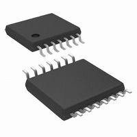
LM3429MH/NOPB National Semiconductor, LM3429MH/NOPB Datasheet - Page 13

LM3429MH/NOPB
Manufacturer Part Number
LM3429MH/NOPB
Description
IC LED DRVR HP CONS CURR 14TSSOP
Manufacturer
National Semiconductor
Series
PowerWise®r
Type
High Power, Constant Currentr
Datasheet
1.LM3429MHNOPB.pdf
(34 pages)
Specifications of LM3429MH/NOPB
Constant Current
Yes
Topology
PWM, SEPIC, Step-Down (Buck), Step-Up (Boost)
Number Of Outputs
1
Internal Driver
No
Type - Primary
Automotive
Type - Secondary
High Brightness LED (HBLED)
Frequency
2MHz
Voltage - Supply
4.5 V ~ 75 V
Mounting Type
Surface Mount
Package / Case
14-TSSOP Exposed Pad, 14-eTSSOP 14-HTSSOP
Operating Temperature
-40°C ~ 125°C
Current - Output / Channel
1A
Internal Switch(s)
No
Efficiency
95%
For Use With
LM3429BSTEVAL - BOARD EVAL FOR BOOST LM3429LM3429BKBSTEVAL - BOARD EVAL FOR BUCK-BOOST LM3429
Lead Free Status / RoHS Status
Lead free / RoHS Compliant
Voltage - Output
-
Other names
LM3429MH
Available stocks
Company
Part Number
Manufacturer
Quantity
Price
INPUT UNDER-VOLTAGE LOCKOUT (UVLO)
The nDIM pin is a dual-function input that features an accurate
1.24V threshold with programmable hysteresis as shown in
Figure
for the LEDs and as a V
and exceeds the 1.24V threshold, 20 µA (typical) of current is
driven out of the nDIM pin into the resistor divider providing
programmable hysteresis.
When using the nDIM pin for UVLO and PWM dimming con-
currently, the UVLO circuit can have an extra series resistor
to set the hysteresis. This allows the standard resistor divider
to have smaller resistor values minimizing PWM delays due
to a pull-down MosFET at the nDIM pin (see PWM Dimming
section). In general, at least 3V of hysteresis is necessary
when PWM dimming if operating near the UVLO threshold.
The turn-on threshold (V
The hysteresis (V
UVLO only
PWM dimming and UVLO
PWM DIMMING
The active low nDIM pin can be driven with a PWM signal
which controls the main NFET (Q1). The brightness of the
LEDs can be varied by modulating the duty cycle of this signal.
LED brightness is approximately proportional to the PWM
signal duty cycle, so 30% duty cycle equals approximately
30% LED brightness. This function can be ignored if PWM
dimming is not required by using nDIM solely as a V
input as described in the Input Under-Voltage Lockout section
or by tying it directly to V
12. This pin functions as both the PWM dimming input
FIGURE 12. UVLO Circuit
HYS
) is defined as follows:
IN
TURN-ON
CC
UVLO. When the pin voltage rises
or V
IN
) is defined as follows:
(if less than 76VDC).
IN
UVLO
300944a5
13
Figure 13
the nDIM pin:
1.
2.
A minimum on-time must be maintained in order for PWM
dimming to operate in the linear region of its transfer function.
Because the controller is disabled during dimming, the PWM
pulse must be long enough such that the energy intercepted
from the input is greater than or equal to the energy being put
into the LEDs. For boost and buck-boost regulators, the fol-
lowing condition must be maintained:
In the previous equation, t
in seconds.
STARTUP REGULATOR (V
The LM3429 includes a high voltage, low dropout (LDO) bias
regulator. When power is applied, the regulator is enabled
and sources current into an external capacitor connected to
the V
supply is internally current limited to 20 mA (minimum). The
recommended bypass capacitance range for the V
tor is 2.2 µF to 3.3 µF. The output of the V
monitored by an internal UVLO circuit that protects the device
during startup, normal operation, and shutdown from attempt-
ing to operate with insufficient supply voltage.
THERMAL SHUTDOWN
The LM3429 includes thermal shutdown. If the die tempera-
ture reaches approximately 165°C the device will shut down
(GATE pin low), until it reaches approximately 140°C where
it turns on again.
Connect the dimming MosFET (Q
the nDIM pin and the source to GND. Apply an external
logic-level PWM signal to the gate of Q
resistor may be necessary to properly turn off Q
signal is present.
Connect the anode of a Schottky diode (D
nDIM pin. Apply an external inverted logic-level PWM
signal to the cathode of the same diode.
CC
pin. The V
shows two ways the PWM signal can be applied to
FIGURE 13. PWM Dimming Circuit
CC
output voltage is 6.9V nominally and the
PULSE
CC
is the length of the PWM pulse
LDO)
DIM
) with the drain to
DIM
CC
300944a6
. A pull down
DIM
www.national.com
regulator is
) to the
CC
DIM
regula-
if no


