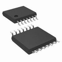
LM3429MH/NOPB National Semiconductor, LM3429MH/NOPB Datasheet - Page 15

LM3429MH/NOPB
Manufacturer Part Number
LM3429MH/NOPB
Description
IC LED DRVR HP CONS CURR 14TSSOP
Manufacturer
National Semiconductor
Series
PowerWise®r
Type
High Power, Constant Currentr
Datasheet
1.LM3429MHNOPB.pdf
(34 pages)
Specifications of LM3429MH/NOPB
Constant Current
Yes
Topology
PWM, SEPIC, Step-Down (Buck), Step-Up (Boost)
Number Of Outputs
1
Internal Driver
No
Type - Primary
Automotive
Type - Secondary
High Brightness LED (HBLED)
Frequency
2MHz
Voltage - Supply
4.5 V ~ 75 V
Mounting Type
Surface Mount
Package / Case
14-TSSOP Exposed Pad, 14-eTSSOP 14-HTSSOP
Operating Temperature
-40°C ~ 125°C
Current - Output / Channel
1A
Internal Switch(s)
No
Efficiency
95%
For Use With
LM3429BSTEVAL - BOARD EVAL FOR BOOST LM3429LM3429BKBSTEVAL - BOARD EVAL FOR BUCK-BOOST LM3429
Lead Free Status / RoHS Status
Lead free / RoHS Compliant
Voltage - Output
-
Other names
LM3429MH
Available stocks
Company
Part Number
Manufacturer
Quantity
Price
N-CHANNEL MosFET (NFET)
The LM3429 requires an external NFET (Q1) as the main
power MosFET for the switching regulator. Q1 is recommend-
ed to have a voltage rating at least 15% higher than the
maximum transistor voltage to ensure safe operation during
the ringing of the switch node. In practice, all switching regu-
lators have some ringing at the switch node due to the diode
parasitic capacitance and the lead inductance. The current
rating is recommended to be at least 10% higher than the
average transistor current. The power rating is then verified
by calculating the power loss given the RMS transistor current
and the NFET on-resistance (R
In general, the NFET should be chosen to minimize total gate
charge (Q
minimize R
power losses in the system. Frequently, higher current NFETs
in larger packages are chosen for better thermal perfor-
mance.
RE-CIRCULATING DIODE
A re-circulating diode (D1) is required to carry the inductor
current during t
Schottky diode due to low forward voltage drop and near-zero
reverse recovery time. Similar to Q1, D1 is recommended to
have a voltage rating at least 15% higher than the maximum
transistor voltage to ensure safe operation during the ringing
of the switch node and a current rating at least 10% higher
than the average diode current. The power rating is verified
by calculating the power loss through the diode. This is ac-
complished by checking the typical diode forward voltage
from the I-V curve on the product datasheet and multiplying
by the average diode current. In general, higher current
diodes have a lower forward voltage and come in better per-
forming packages minimizing both power losses and temper-
ature rise.
g
) whenever switching frequencies are high and
DS-ON
OFF
otherwise. This will minimize the dominant
. The most efficient choice for D1 is a
DS-ON
).
15
CIRCUIT LAYOUT
The performance of any switching regulator depends as much
upon the layout of the PCB as the component selection. Fol-
lowing a few simple guidelines will maximimize noise rejection
and minimize the generation of EMI within the circuit.
Discontinuous currents are the most likely to generate EMI,
therefore care should be taken when routing these paths. The
main path for discontinuous current in the LM3429 buck reg-
ulator contains the input capacitor (C
diode (D1), the N-channel MosFET (Q1), and the sense re-
sistor (R
the discontinuous current flows through the output capacitor
(C
as small as possible and the connections between all the
components should be short and thick to minimize parasitic
inductance. In particular, the switch node (where L1, D1 and
Q1 connect) should be just large enough to connect the com-
ponents. To minimize excessive heating, large copper pours
can be placed adjacent to the short current path of the switch
node.
The RCT, COMP, CSH, IS, HSP and HSN pins are all high-
impedance inputs which couple external noise easily, there-
fore the loops containing these nodes should be minimized
whenever possible.
In some applications the LED or LED array can be far away
(several inches or more) from the LM3429, or on a separate
PCB connected by a wiring harness. When an output capac-
itor is used and the LED array is large or separated from the
rest of the regulator, the output capacitor should be placed
close to the LEDs to reduce the effects of parasitic inductance
on the AC impedance of the capacitor.
O
), D1, Q1, and R
LIM
). In the LM3429 boost and buck-boost regulators,
LIM
. In either case, this loop should be kept
IN
), the recirculating
www.national.com


