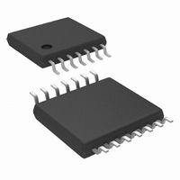
LM3429MH/NOPB National Semiconductor, LM3429MH/NOPB Datasheet - Page 3

LM3429MH/NOPB
Manufacturer Part Number
LM3429MH/NOPB
Description
IC LED DRVR HP CONS CURR 14TSSOP
Manufacturer
National Semiconductor
Series
PowerWise®r
Type
High Power, Constant Currentr
Datasheet
1.LM3429MHNOPB.pdf
(34 pages)
Specifications of LM3429MH/NOPB
Constant Current
Yes
Topology
PWM, SEPIC, Step-Down (Buck), Step-Up (Boost)
Number Of Outputs
1
Internal Driver
No
Type - Primary
Automotive
Type - Secondary
High Brightness LED (HBLED)
Frequency
2MHz
Voltage - Supply
4.5 V ~ 75 V
Mounting Type
Surface Mount
Package / Case
14-TSSOP Exposed Pad, 14-eTSSOP 14-HTSSOP
Operating Temperature
-40°C ~ 125°C
Current - Output / Channel
1A
Internal Switch(s)
No
Efficiency
95%
For Use With
LM3429BSTEVAL - BOARD EVAL FOR BOOST LM3429LM3429BKBSTEVAL - BOARD EVAL FOR BUCK-BOOST LM3429
Lead Free Status / RoHS Status
Lead free / RoHS Compliant
Voltage - Output
-
Other names
LM3429MH
Available stocks
Company
Part Number
Manufacturer
Quantity
Price
STARTUP REGULATOR (V
V
I
I
V
V
OVER-VOLTAGE PROTECTION (OVP)
V
I
ERROR AMPLIFIER
V
OFF TIMER (RCT)
t
R
V
CC-LIM
Q
HYS-OVP
OFF-MIN
CC-REG
CC-UVLO
CC-HYS
TH-OVP
CSH
RCT
RCT
Absolute Maximum Ratings
If Military/Aerospace specified devices are required,
please contact the National Semiconductor Sales Office/
Distributors for availability and specifications.
Electrical Characteristics
Specifications in standard type face are for T
Range ( T
values represent the most likely parametric norm at T
stated the following condition applies: V
V
OVP, HSP, HSN
RCT
IS
V
COMP, CSH
GATE
Symbol
IN
CC
, nDIM
J
= −40°C to +125°C). Minimum and Maximum limits are guaranteed through test, design, or statistical correlation. Typical
V
V
Quiescent Current
V
V
OVP OVLO Threshold
OVP Hysteresis Source
Current
CSH Reference Voltage
Error Amplifier Input Bias
Current
COMP Sink / Source
Current
Transconductance
Linear Input Range
Transconductance
Bandwidth
Minimum Off-time
RCT Reset Pull-down
Resistance
V
CC
CC
CC
CC
IN
/25 Reference Voltage
Regulation
Current Limit
UVLO Threshold
UVLO Hysteresis
Parameter
CC
)
-1 mA to +5 mA continuous
-1 mA to +1 mA continuous
V
IN
-100 µA continuous
-200 µA to +200 µA
CC
-1 mA continuous
-1 mA continuous
= +14V.
+2.5V for 100 ns
-2.5V for 100 ns
I
V
Static
V
V
OVP Increasing
OVP Active (high)
With Respect to AGND
(Note
-6dB Unloaded Response
(Note
RCT = 1V through 1 kΩ
V
CC
(Note
J
-0.3V to 76.0V
-0.3V to 76.0V
-0.3V to 76.0V
-2V for 100 ns
CC
CC
CC
IN
-0.3V to 3.0V
-0.3V to 8.0V
-0.3V to 6.0V
= 25°C and those with boldface type apply over the full Operating Temperature
-0.3V to V
= 0 mA
= 14V
(Note
Continuous
= 0V
Increasing
Decreasing
7)
7)
1)
Conditions
J
1)
= +25°C, and are provided for reference purposes only. Unless otherwise
CC
3
Operating Conditions
PGND
Maximum Junction
Temperature
Storage Temperature Range
Maximum Lead Temperature
(Reflow and Solder)
Continuous Power Dissipation
ESD Susceptibility
Operating Junction
Temperature Range
Input Voltage V
Human Body Model
(Note
1.180
1.210
6.30
3.70
Min
-0.6
540
0.5
20
10
10
5)
IN
(Note
(Note
(Note
1.240
1.235
±125
6.90
4.17
4.08
Typ
100
565
4)
1.6
0.1
1.0
27
20
26
35
36
0
3)
6)
-2.5V to 2.5V for 100 ns
(Note
(Note
1.280
1.260
Max
7.35
4.50
120
585
3.0
0.6
30
40
75
−65°C to +150°C
−40°C to +125°C
Internally Limited
Internally Limited
1)
5)
-0.3V to 0.3V
4.5V to 75V
www.national.com
260°C
Units
2 kV
µA/V
MHz
mA
mV
mV
µA
µA
ns
V
V
V
V
Ω


