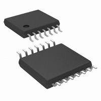
LM3429MH/NOPB National Semiconductor, LM3429MH/NOPB Datasheet - Page 4

LM3429MH/NOPB
Manufacturer Part Number
LM3429MH/NOPB
Description
IC LED DRVR HP CONS CURR 14TSSOP
Manufacturer
National Semiconductor
Series
PowerWise®r
Type
High Power, Constant Currentr
Datasheet
1.LM3429MHNOPB.pdf
(34 pages)
Specifications of LM3429MH/NOPB
Constant Current
Yes
Topology
PWM, SEPIC, Step-Down (Buck), Step-Up (Boost)
Number Of Outputs
1
Internal Driver
No
Type - Primary
Automotive
Type - Secondary
High Brightness LED (HBLED)
Frequency
2MHz
Voltage - Supply
4.5 V ~ 75 V
Mounting Type
Surface Mount
Package / Case
14-TSSOP Exposed Pad, 14-eTSSOP 14-HTSSOP
Operating Temperature
-40°C ~ 125°C
Current - Output / Channel
1A
Internal Switch(s)
No
Efficiency
95%
For Use With
LM3429BSTEVAL - BOARD EVAL FOR BOOST LM3429LM3429BKBSTEVAL - BOARD EVAL FOR BUCK-BOOST LM3429
Lead Free Status / RoHS Status
Lead free / RoHS Compliant
Voltage - Output
-
Other names
LM3429MH
Available stocks
Company
Part Number
Manufacturer
Quantity
Price
www.national.com
PWM COMPARATOR
CURRENT LIMIT (IS)
V
t
HIGH SIDE TRANSCONDUCTANCE AMPLIFIER
GATE DRIVER (GATE)
R
R
UNDER-VOLTAGE LOCKOUT and DIM INPUT (nDIM)
V
I
THERMAL SHUTDOWN
T
T
THERMAL RESISTANCE
θ
θ
ON-MIN
HYS-nDIM
SD
HYS
JA
JC
LIM
TH-nDIM
SRC(GATE)
SNK(GATE)
Note 1: Absolute Maximum Ratings indicate limits beyond which damage to the device may occur, including inoperability and degradation of device reliability
and/or performance. Functional operation of the device and/or non-degradation at the Absolute Maximum Ratings or other conditions beyond those indicated in
the Operating Ratings is not implied. The recommended Operating Ratings indicate conditions at which the device is functional and the device should not be
operated beyond such conditions. All voltages are with respect to the potential at the AGND pin, unless otherwise specified.
Note 2: Junction-to-ambient thermal resistance is highly board-layout dependent. The numbers listed in the table are given for a reference layout wherein the
14L TSSOP EP package has its DAP pad populated with 9 vias. In applications where high maximum power dissipation exists, namely driving a large MosFET
at high switching frequency from a high input voltage, special care must be paid to thermal dissipation issues during board design. In high-power dissipation
applications, the maximum ambient temperature may have to be derated. Maximum ambient temperature (T
junction temperature (T
of the package in the application (θ
power dissipation capability of this advanced package. Under these circumstances, no vias would be required and the thermal resistances would be 104 °C/W
for the 14L TSSOP EP. It is possible to conservatively interpolate between the full via count thermal resistance and the no via count thermal resistance with a
straight line to get a thermal resistance for any number of vias in between these two limits.
Note 3: Refer to National’s packaging website for more detailed information and mounting techniques. http://www.national.com/analog/packaging/
Note 4: Human Body Model, applicable std. JESD22-A114-C.
Note 5: All limits guaranteed at room temperature (standard typeface) and at temperature extremes (bold typeface). All room temperature limits are 100%
production tested. All limits at temperature extremes are guaranteed via correlation using standard Statistical Quality Control (SQC) methods. All limits are used
to calculate Average Outgoing Quality Level (AOQL).
Note 6: Typical numbers are at 25°C and represent the most likely norm.
Note 7: These electrical parameters are guaranteed by design, and are not verified by test.
Note 8: The measurements were made using the standard buck-boost evaluation board from AN-1985.
Note 9: The measurements were made using the standard boost evaluation board from AN-1986.
Symbol
COMP to PWM Offset
Current Limit Threshold
V
Leading Edge Blanking
Time
Input Bias Current
Transconductance
Input Offset Current
Input Offset Voltage
Transconductance
Bandwidth
GATE Sourcing Resistance GATE = High
GATE Sinking Resistance
nDIM / UVLO Threshold
nDIM Hysteresis Current
Thermal Shutdown
Threshold
Thermal Shutdown
Hysteresis
Junction to Ambient
(Note
Junction to Exposed Pad
(DAP)
LIM
J-MAX-OP
Delay to Output
2)
Parameter
= 125°C), the maximum power dissipation of the device in the application (P
JA
), as given by the following equation: T
I
(Note
GATE = Low
(Note
(Note
14L TSSOP EP
14L TSSOP EP
CSH
= 100 µA
7)
7)
7)
Conditions
A-MAX
4
= T
J-MAX-OP
– (θ
(Note
JA
1.180
Min
700
215
-1.5
250
× P
75
20
10
-7
D-MAX
5)
D-MAX
A-MAX
). In most applications there is little need for the full
), and the junction-to ambient thermal resistance
) is dependent on the maximum operating
(Note
1.240
Typ
800
245
250
119
500
165
2.0
1.3
5.5
35
10
20
25
40
0
0
6)
(Note
1.280
Max
900
275
450
1.5
6.0
4.5
75
30
7
5)
Units
mA/V
°C/W
°C/W
kHz
mV
mV
mV
µA
µA
µA
°C
ns
Ω
V


