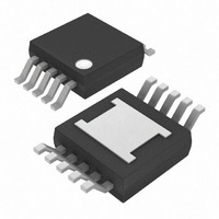
MAX7306AUB+ Maxim Integrated Products, MAX7306AUB+ Datasheet - Page 10

MAX7306AUB+
Manufacturer Part Number
MAX7306AUB+
Description
IC LED DRIVER LINEAR 10-UMAX
Manufacturer
Maxim Integrated Products
Type
Linear (I²C Interface)r
Datasheet
1.MAX7306AUB.pdf
(23 pages)
Specifications of MAX7306AUB+
Topology
PWM
Number Of Outputs
4
Internal Driver
Yes
Type - Primary
Backlight, LED Blinker
Type - Secondary
White LED
Frequency
1MHz
Voltage - Supply
1.62 V ~ 3.6 V
Mounting Type
Surface Mount
Package / Case
10-MSOP Exposed Pad, 10-HMSOP, 10-eMSOP
Operating Temperature
-40°C ~ 125°C
Current - Output / Channel
25mA
Internal Switch(s)
No
Lead Free Status / RoHS Status
Lead free / RoHS Compliant
Voltage - Output
-
Efficiency
-
Lead Free Status / Rohs Status
Details
SMBus/I
GPIOs and LED Drivers
The MAX7307 is set to slave address 0x98 and the
MAX7306 can be set to one of four I
0x98 to 0x9F, using the address input AD0 (see Table 5)
and is accessed over an I
The MAX7306 slave address is determined on each I
transmission, regardless of the transmission actually
addressing the device or not. The MAX7306 distin-
guishes whether address input AD0 is connected to
SDA, SCL, V
Therefore, the MAX7306 slave address can be config-
ured dynamically in an application without toggling the
device supply.
Table 5. Slave-Address Selection
Table 6. Port I/O Registers (I/O Port Set as an Input, Registers 0x01 to 0x04)
*Bit D6 controls the I/O’s supply reference for the MAX7307. The MAX7306 ignores bit D6.
10
C O NN EC TIO N
REGISTER BIT
GND
AD0
SDA
V
SCL
______________________________________________________________________________________
DD
D4, D3
D6*
D7
D5
D2
D1
D0
DD
A6
1
1
1
1
, or GND during the transmission.
2
Transition Interrupt
A5
State (Read-Only)
0
0
0
0
DESCRIPTION
Port I/O Set Bit
Port Transition
C Interfaced 4-Port, Level-Translating
(Read-Only)
Port Supply
Port Status
Reference
Debounce
Reserved
Enable
A4
DEVICE ADDRESS
0
0
0
0
2
C or SMBus serial interface.
A3
1
1
1
1
A2
2
1
1
1
1
Slave Address
C slave addresses
VALUE
A1
0
0
1
1
1
0
1
0
1
0
0
1
0
1
0
1
A0
0
1
0
1
Sets the I/O port as an input.
Refers the input to the V
Refers the input to the V
Disables the transition interrupt.
Enables the transition interrupt.
Do not write to these registers.
Disables debouncing of the input port.
Enables debouncing of the input port.
No transition has occurred since the last port read.
A transition has occurred since the last port read.
Port input is logic-low.
Port input is logic-high.
R /W
0/1
0/1
0/1
0/1
2
C
The port I/O registers set the I/O ports, one register per
port (see Tables 6 and 7). Use the I/O port registers to
configure the ports individually as inputs, open-drain, or
push-pull outputs. Port P1 can only be configured as an
input or an open-drain output. The push-pull bit (D6) set-
ting for the port I/O register P1 is ignored.
Configure a port as an input by writing a logic-high to the
MSB (bit D7) of the port I/O register (see Table 6). To
obtain the logic level of the port input, read the port I/O
register bit, D0. This readback value is the instantaneous
logic level at the time of the read request if debounce is
disabled for the port (port I/O register bit D2 = 0), or the
debounced result if debounce is enabled for the port
(port I/O register bit D2 = 1). See Figure 1 for input port
structure.
Configure a port as an output by writing a logic-low to the
MSB (bit D7) of the port I/O register. The device reads
back the logic level, PWM, or the blink setting of the port
(see Table 7).
LA
DD
supply voltage.
supply voltage.
FUNCTION
I/O Port Registers
I/O Output Port
I/O Input Port


