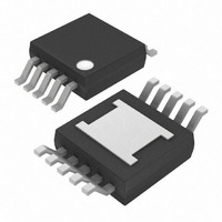
MAX7306AUB+ Maxim Integrated Products, MAX7306AUB+ Datasheet - Page 19

MAX7306AUB+
Manufacturer Part Number
MAX7306AUB+
Description
IC LED DRIVER LINEAR 10-UMAX
Manufacturer
Maxim Integrated Products
Type
Linear (I²C Interface)r
Datasheet
1.MAX7306AUB.pdf
(23 pages)
Specifications of MAX7306AUB+
Topology
PWM
Number Of Outputs
4
Internal Driver
Yes
Type - Primary
Backlight, LED Blinker
Type - Secondary
White LED
Frequency
1MHz
Voltage - Supply
1.62 V ~ 3.6 V
Mounting Type
Surface Mount
Package / Case
10-MSOP Exposed Pad, 10-HMSOP, 10-eMSOP
Operating Temperature
-40°C ~ 125°C
Current - Output / Channel
25mA
Internal Switch(s)
No
Lead Free Status / RoHS Status
Lead free / RoHS Compliant
Voltage - Output
-
Efficiency
-
Lead Free Status / Rohs Status
Details
recipients. When the MAX7306/MAX7307 transmit to the
master, the master generates the acknowledge bit
because the master is the recipient.
The MAX7306/MAX7307 have a 7-bit long slave
address (Figure 12). The 8th bit following the 7-bit slave
address is the R/W bit. Set the R/W bit low for a write
command and high for a read command.
The first 5 bits of the MAX7306 slave address (A6–A2)
are always 1, 0, 0, 1, and 1. Slave address bits A1 and
A0 are selected by the address input AD0. AD0 can be
connected to GND, V
has four possible slave addresses (see Table 5), and
therefore, a maximum of four MAX7306 devices can be
controlled independently from the same interface. The
MAX7307 features a permanent slave address of 0x98.
Figure 11. Acknowledge
Figure 12. Slave Address
Figure 13. Register Address Received
TRANSMITTER
SMBus/I
RECEIVER
SDA BY
SDA BY
SDA
SCL
SCL
CONDITION
START
S
MSB
1
S
______________________________________________________________________________________
1
2
DD
C Interfaced 4-Port, Level-Translating
, SDA, or SCL. The MAX7306
0
2
SLAVE ADDRESS
FOR ACKNOWLEDGE
ACKNOWLEDGE FROM MAX7306
CLOCK PULSE
0
Slave Address
8
R/W
1
9
0
A
1
D15
A write to the MAX7306/MAX7307 comprises the trans-
mission of the MAX7306/MAX7307’s slave address with
the R/W bit set to zero, followed by at least 1 byte of
information. The first byte of information is the command
byte. The command byte determines which register of
the MAX7306/MAX7307 is to be written to by the next
byte, if received (see Table 1). If a STOP condition is
detected after the command byte is received, the
MAX7306/MAX7307 take no further action beyond stor-
ing the command byte (see Figure 13).
Any bytes received after the command byte are data
bytes. The first data byte goes into the internal register of
the MAX7306/MAX7307 selected by the command byte
(see Figure 14). If multiple data bytes are transmitted
before a STOP condition is detected, these bytes are
generally stored in subsequent MAX7306/MAX7307
internal registers because the command byte address
autoincrements (see Table 1).
The MAX7306/MAX7307 are read using the MAX7306/
MAX7307’s internally stored command byte as an
address pointer the same way the stored command byte
is used as an address pointer for a write. The pointer
autoincrements after each data byte is read using the
GPIOs and LED Drivers
Message Format for Writing to the MAX7306/MAX7307
D14
D13
1
REGISTER ADDRESS
D12
ACKNOWLEDGE FROM MAX7306
D11
LSB
A0
D10
D9
Message Format for Reading
D8
R/W
A
P
ACK
19


