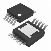
MAX7306AUB+ Maxim Integrated Products, MAX7306AUB+ Datasheet - Page 4

MAX7306AUB+
Manufacturer Part Number
MAX7306AUB+
Description
IC LED DRIVER LINEAR 10-UMAX
Manufacturer
Maxim Integrated Products
Type
Linear (I²C Interface)r
Datasheet
1.MAX7306AUB.pdf
(23 pages)
Specifications of MAX7306AUB+
Topology
PWM
Number Of Outputs
4
Internal Driver
Yes
Type - Primary
Backlight, LED Blinker
Type - Secondary
White LED
Frequency
1MHz
Voltage - Supply
1.62 V ~ 3.6 V
Mounting Type
Surface Mount
Package / Case
10-MSOP Exposed Pad, 10-HMSOP, 10-eMSOP
Operating Temperature
-40°C ~ 125°C
Current - Output / Channel
25mA
Internal Switch(s)
No
Lead Free Status / RoHS Status
Lead free / RoHS Compliant
Voltage - Output
-
Efficiency
-
Lead Free Status / Rohs Status
Details
SMBus/I
GPIOs and LED Drivers
PORT, INTERRUPT (INT), AND RESET (RST) TIMING CHARACTERISTICS
(V
+25°C.) (Note 1) (See Figures 14, 15, and 16)
TIMING CHARACTERISTICS
(V
+25°C.) (Note 1) (See Figure 8)
Note 1: All parameters are tested at T
Note 2: Guaranteed by design.
Note 3: A master device must provide a hold time of at least 300ns for the SDA signal (referred to V
Note 4: C
Note 5: Input filters on the SDA and SCL inputs suppress noise spikes less than 50ns.
4
Oscillator Frequency
Port Output Data Valid High Time
Port Output Data Valid Low Time (Internal or
External Oscillator Running)
Port Output Data Valid Low Time (Oscillator Not
Running)
Port Input Setup Time
Port Input Hold Time
INT Input Data Valid Time
INT Reset Delay Time from Acknowledge
RST Pulse Width
RST Rising to START Condition Setup Time
Serial-Clock Frequency
Bus Timeout
Bus Fr ee Tim e Betw een a S TOP and a S TART C ond i ti on
Hold Time, (Repeated) START Condition
Repeated START Condition Setup Time
STOP Condition Setup Time
Data Hold Time
Data Setup Time
SCL Clock Low Period
SCL Clock High Period
Rise Time of Both SDA and SCL Signals, Receiving
Fall Time of Both SDA and SCL Signals, Receiving
Fall Time of SDA Transmitting
Pulse Width of Spike Suppressed
C ap aci ti ve Load for E ach Bus Li ne
DD
DD
_______________________________________________________________________________________
= 1.62V to 3.6V, T
= 1.62V to 3.6V, T
undefined region of SCL’s falling edge.
b
= total capacitance of one bus line in pF. t
PARAMETER
PARAMETER
2
A
A
= T
= T
C Interfaced 4-Port, Level-Translating
MIN
MIN
to T
to T
MAX
MAX
A
= +25°C. Specifications over temperature are guaranteed by design.
, unless otherwise noted. Typical values are at V
, unless otherwise noted. Typical values are at V
R
SYMBOL
SYMBOL
t
TIMEOUT
t
t
t
t
t
and t
t
t
HD,DAT
HD,STA
SU,STO
SU,DAT
t
SU,STA
t
PPVL1
PPVL2
t
f
PPVH
t
t
t
t
f
HIGH
LOW
CLK
PSU
t
BUF
F.TX
RST
SCL
t
t
C
t
t
PH
t
t
SP
IR
IV
W
R
F
b
F
are measured between 0.3 x V
f
f
C
C
C
C
C
C
C
(Note 3)
(Notes 2, 4)
(Notes 2, 4)
(Note 4)
(Note 5)
(Note 2)
CLK
CLK
L
L
L
L
L
L
L
≤ 100pF
≤ 100pF (Note 2)
≤ 100pF
= 100pF
= 100pF
= 100pF
= 100pF
= internal oscillator
= external input
CONDITIONS
CONDITIONS
DD
DD
= 3.3V, V
= 3.3V, V
DD
and 0.7 x V
MIN
500
900
MIN
100
1.3
0.6
0.6
0.6
1.3
0.7
0
4
IL
LA
LA
of the SCL signal) to bridge the
20 + 0.1C
20 + 0.1C
20 + 0.1C
= 3.3V (MAX7307 only), T
= 3.3V (MAX7307 only), T
TYP
TYP
32
40
DD
31
50
.
b
b
b
1 / f
MAX
MAX
400
300
300
250
400
0.9
1
4
4
4
CLK
UNITS
UNITS
MHz
kHz
kHz
ms
pF
µs
µs
µs
µs
µs
ns
µs
µs
ns
ns
ns
ns
µs
µs
µs
µs
ns
ns
µs
µs
µs
A
A
=
=


