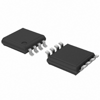
PCA9632DP1,118 NXP Semiconductors, PCA9632DP1,118 Datasheet - Page 15

PCA9632DP1,118
Manufacturer Part Number
PCA9632DP1,118
Description
IC LED DRIVER RGBA 8-TSSOP
Manufacturer
NXP Semiconductors
Type
RGBA LED Driverr
Datasheet
1.PCA9632TK118.pdf
(38 pages)
Specifications of PCA9632DP1,118
Package / Case
8-TSSOP
Topology
Open Drain, PWM
Number Of Outputs
4
Internal Driver
Yes
Type - Primary
Backlight, LED Blinker
Type - Secondary
RGBA
Frequency
1MHz
Voltage - Supply
2.3 V ~ 5.5 V
Voltage - Output
5.5V
Mounting Type
Surface Mount
Operating Temperature
-40°C ~ 85°C
Current - Output / Channel
25mA
Internal Switch(s)
Yes
Number Of Segments
4
Low Level Output Current
100000 uA
Operating Supply Voltage
2.3 V to 5.5 V
Maximum Supply Current
150 uA
Maximum Power Dissipation
400 mW
Maximum Operating Temperature
+ 85 C
Mounting Style
SMD/SMT
Minimum Operating Temperature
- 40 C
Lead Free Status / RoHS Status
Lead free / RoHS Compliant
Efficiency
-
Lead Free Status / Rohs Status
Lead free / RoHS Compliant
Other names
935284899118
PCA9632DP1-T
PCA9632DP1-T
PCA9632DP1-T
PCA9632DP1-T
Available stocks
Company
Part Number
Manufacturer
Quantity
Price
Part Number:
PCA9632DP1,118
Manufacturer:
NXP/恩智浦
Quantity:
20 000
NXP Semiconductors
PCA9632_3
Product data sheet
7.3.8 LED All Call I
7.4 Power-on reset
7.5 Software reset
Once subaddresses have been programmed to their right values, SUBx bits need to be
set to 1 in order to have the device acknowledging these addresses (MODE1 register).
Only the 7 MSBs representing the I
register is a read-only bit (0).
When SUBx is set to 1, the corresponding I
an I
Table 13.
Legend: * default value.
The LED All Call I
at the same time (ALLCALL bit in register MODE1 must be equal to 1, power-up default
state). This address is programmable through the I
an I
sub call.
Only the 7 MSBs representing the All Call I
ALLCALLADR register is a read-only bit (0).
If ALLCALL bit = 0, the device does not acknowledge the address programmed in register
ALLCALLADR.
When power is applied to V
condition until V
PCA9632 registers and I
zeroes) causing all the channels to be deselected. Thereafter, V
0.2 V to reset the device.
The Software Reset Call (SWRST Call) allows all the devices in the I
the power-up state value through a specific formatted I
correctly, it implies that the I
bus.
The SWRST Call function is defined as the following:
Address
0Ch
1. A START command is sent by the I
2. The reserved SWRST I
3. The PCA9632 device(s) acknowledge(s) after seeing the SWRST Call address
2
2
sent by the I
‘0000 0110’ (06h) only. If the R/W bit is set to 1 (read), no acknowledge is returned to
the I
C-bus read or write sequence.
C-bus read or write sequence. The register address can be programmed as a
2
C-bus master.
Register
ALLCALLADR
ALLCALLADR - LED All Call I
description
2
DD
2
C-bus address, ALLCALLADR
C-bus master.
2
C-bus address allows all the PCA9632s in the bus to be programmed
has reached V
Rev. 03 — 15 July 2008
2
C-bus state machine are initialized to their default states (all
Bit
7:1
0
DD
2
2
C-bus address ‘0000 011’ with the R/W bit set to 0 (write) is
C-bus is functional and that there is no device hanging the
, an internal power-on reset holds the PCA9632 in a reset
Symbol
AC[7:1]
AC[0]
POR
2
C-bus subaddress are valid. The LSB in SUBADRx
. At this point, the reset condition is released and the
2
2
C-bus address register (address 0Ch) bit
C-bus master.
2
2
Access Value
R/W
R only
C-bus address are valid. The LSB in
C-bus subaddress can be used during either
4-bit Fm+ I
2
C-bus and can be used during either
1110 000*
0*
2
C-bus command. To be performed
2
C-bus low power LED driver
DD
Description
ALLCALL I
address register
reserved
must be lowered below
2
C-bus to be reset to
PCA9632
© NXP B.V. 2008. All rights reserved.
2
C-bus
15 of 38


