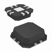
ISL6208ACRZ Intersil, ISL6208ACRZ Datasheet - Page 3

ISL6208ACRZ
Manufacturer Part Number
ISL6208ACRZ
Description
IC MOSFET DRVR SYNC BUCK 8-QFN
Manufacturer
Intersil
Datasheet
1.ISL6208ACBZ.pdf
(10 pages)
Specifications of ISL6208ACRZ
Configuration
High and Low Side, Synchronous
Input Type
PWM
Delay Time
26ns
Current - Peak
2A
Number Of Configurations
1
Number Of Outputs
2
High Side Voltage - Max (bootstrap)
33V
Voltage - Supply
4.5 V ~ 5.5 V
Operating Temperature
-10°C ~ 100°C
Mounting Type
Surface Mount
Package / Case
8-VQFN
Lead Free Status / RoHS Status
Lead free / RoHS Compliant
Absolute Maximum Ratings
Supply Voltage (VCC) . . . . . . . . . . . . . . . . . . . . . . . . . . -0.3V to 7V
Input Voltage (V
BOOT Voltage (V
BOOT To PHASE Voltage (V
PHASE Voltage (Note 1) . . . . . . . . . . . . . . . . . . . GND - 0.3V to 30V
UGATE Voltage . . . . . . . . . . . . . . . . V
LGATE Voltage . . . . . . . . . . . . . . . GND - 0.3V (DC) to VCC + 0.3V
Ambient Temperature Range . . . . . . . . . . . . . . . . . . .-40°C to 125°C
Recommended Operating Conditions
Ambient Temperature Range . . . . . . . . . . . . . . . . . . .-10°C to 100°C
Maximum Operating Junction Temperature. . . . . . . . . . . . . . 125°C
Supply Voltage, VCC . . . . . . . . . . . . . . . . . . . . . . . . . . . . . 5V ±10%
CAUTION: Stresses above those listed in “Absolute Maximum Ratings” may cause permanent damage to the device. This is a stress only rating and operation of the
device at these or any other conditions above those indicated in the operational sections of this specification is not implied.
NOTES:
Electrical Specifications
VCC SUPPLY CURRENT
Bias Supply Current
POR
POR Hysteresis
BOOTSTRAP DIODE
Forward Voltage
PWM INPUT
Input Current
PWM Three-State Rising Threshold
PWM Three-State Falling Threshold
Three-State Shutdown Holdoff Time
UG/LG Three-state Propagation Delay
FCCM INPUT
FCCM Threshold
FCCM Transient Delay
SWITCHING TIME
UGATE Rise Time (Note 5)
LGATE Rise Time (Note 5)
UGATE Fall Time (Note 5)
1. The Phase Voltage is capable of withstanding -7V DC when the BOOT pin is at GND.
2. θ
3. θ
4. For θ
Tech Brief TB379.
JA
JA
is measured with the component mounted on a high effective thermal conductivity test board in free air. See Tech Brief TB379 for details.
is measured in free air with the component mounted on a high effective thermal conductivity test board with “direct attach” features. See
JC
, the “case temp” location is the center of the exposed metal pad on the package underside.
GND - 2.5V (<20ns Pulse Width, 5µJ) to VCC + 0.3V
PARAMETER
FCCM
V
BOOT-GND
PHASE
, V
PWM
- 5V (<20ns Pulse Width, 10µJ) to V
). . . . . . . . . . . . . . . . . . . . . -0.3V to 33V
BOOT-PHASE
). . . . . . . . . . . . . -0.3V to VCC + 0.3V
GND -8V (<20ns Pulse Width, 10µJ)
3
Recommended Operating Conditions, Unless Otherwise Noted
PHASE
) . . . . . . -0.3V to 7V (DC)
- 0.3V (DC) to V
-0.3V to 9V (<10ns)
SYMBOL
t
TSSHD
I
I
t
PWM
VCC
t
PTS
t
t
V
RU
FU
RL
F
PWM pin floating, V
Vcc Rising
Vcc Falling
V
V
V
V
V
V
R
V
V
V
BOOT
BOOT
VCC
PWM
PWM
VCC
VCC
VCC
SET
VCC
VCC
VCC
ISL6208A
= 0Ω
= 5V, forward bias current = 2mA
= 5V
= 5V
= 5V, temperature = 25°C
= 5V, 3nF Load
= 5V, 3nF Load
= 5V, 3nF Load
= 5V, V
= 0V, V
TEST CONDITIONS
FCCM
FCCM
Thermal Information
Thermal Resistance (Typical Notes 2, 3, 4) θ
Maximum Junction Temperature (Plastic Package) . . . . . . . . 150°C
Maximum Storage Temperature Range . . . . . . . . . . . -65°C to 150°C
Maximum Lead Temperature (Soldering 10s) . . . . . . . . . . . . . 300°C
SOIC Package (Note 2) . . . . . . . . . . . .
QFN Package (Notes 3, 4). . . . . . . . . .
(SOIC - Lead Tips Only)
FCCM
= 5V
= 5V
= 5V
MIN
2.40
0.45
0.70
3.5
-
-
-
-
-
-
-
-
-
-
-
-
-250
TYP
3.30
2.90
0.60
1.00
100
400
250
3.8
2.5
8.0
8.0
8.0
70
20
70
JA
110
(°C/W)
80
MAX
3.90
0.65
1.30
4.1
-
-
-
-
-
-
-
-
-
-
-
-
February 15, 2006
θ
JC
UNITS
FN9272.0
n/a
(°C/W)
15
mV
µA
µA
µA
ns
ns
ns
ns
ns
ns
V
V
V
V
V
V


