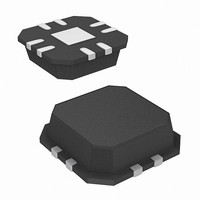
ISL6208ACRZ Intersil, ISL6208ACRZ Datasheet - Page 7

ISL6208ACRZ
Manufacturer Part Number
ISL6208ACRZ
Description
IC MOSFET DRVR SYNC BUCK 8-QFN
Manufacturer
Intersil
Datasheet
1.ISL6208ACBZ.pdf
(10 pages)
Specifications of ISL6208ACRZ
Configuration
High and Low Side, Synchronous
Input Type
PWM
Delay Time
26ns
Current - Peak
2A
Number Of Configurations
1
Number Of Outputs
2
High Side Voltage - Max (bootstrap)
33V
Voltage - Supply
4.5 V ~ 5.5 V
Operating Temperature
-10°C ~ 100°C
Mounting Type
Surface Mount
Package / Case
8-VQFN
Lead Free Status / RoHS Status
Lead free / RoHS Compliant
Diode Emulation
Diode emulation allows for higher converter efficiency under
light-load situations. With diode emulation active, the
ISL6208A will detect the zero current crossing of the output
inductor and turn off LGATE. This ensures that
discontinuous conduction mode (DCM) is achieved. Diode
emulation is asynchronous to the PWM signal. Therefore,
the ISL6208A will respond to the FCCM input immediately
after it changes state. Refer to the waveforms on page 6.
NOTE: Intersil does not recommend DCM mode use with r
current sensing topologies. The turn-OFF of the low side MOSFET
can cause gross current measurement inaccuracies.
Three-State PWM Input
A unique feature of the ISL6208A and other Intersil drivers is
the addition of a shutdown window to the PWM input. If the
PWM signal enters and remains within the shutdown window
for a set holdoff time, the output drivers are disabled and
both MOSFET gates are pulled and held low. The shutdown
state is removed when the PWM signal moves outside the
shutdown window. Otherwise, the PWM rising and falling
thresholds outlined in the ELECTRICAL SPECIFICATIONS
determine when the lower and upper gates are enabled.
Adaptive Shoot-Through Protection
Both drivers incorporate adaptive shoot-through protection
to prevent upper and lower MOSFETs from conducting
simultaneously and shorting the input supply. This is
accomplished by ensuring the falling gate has turned off one
MOSFET before the other is allowed to turn on.
During turn-off of the lower MOSFET, the LGATE voltage is
monitored until it reaches a 1V threshold, at which time the
UGATE is released to rise. Adaptive shoot-through circuitry
monitors the upper MOSFET gate-to-source voltage during
UGATE turn-off. Once the upper MOSFET gate-to-source
voltage has dropped below a threshold of 1V, the LGATE is
allowed to rise.
In addition to gate threshold monitoring, a programmable
delay between MOSFET switching can be accomplished by
placing a resistor in series with the FCCM input. This delay
allows for maximum design flexibility over MOSFET
selection. The delay can be programmed from 5ns to 50ns
above the adaptive shoot-through protection and is obtained
from the absolute value of the current flowing into the FCCM
pin. If no resistor is used, the minimum 5ns delay is used.
Gate threshold monitoring is not affected by the addition or
removal of the additional dead-time. Refer to Figure 8 and
Figure 9 for more detail.
7
DS(ON)
ISL6208A
The equation governing the dead-time seen in Figure 9 is
expressed as:
T
1V
1V
DELAY ns
GATE A
FIGURE 9. ISL6208A PROGRAMMABLE DEAD-TIME vs
GATE A
50
45
40
35
30
25
20
15
10
5
0
(
0
FIGURE 8. PROGRAMMABLE DEAD-TIME
)
=
DELAY RESISTOR
[
167
0.045
FCCM = RESISTOR to VCC or GND
FCCM = VCC or GND
Adaptive Protection with Delay
×
t
delay
R
333
DELAY kΩ
= 5n - 50ns
R
DELAY
Adaptive Shoot-Through Protection
(
500
)
t
(kΩ)
]
DELAY
+
5ns
GATE B
667
833
February 15, 2006
GATE B
FN9272.0
1000


