ISL6208ACRZ Intersil, ISL6208ACRZ Datasheet - Page 5
ISL6208ACRZ
Manufacturer Part Number
ISL6208ACRZ
Description
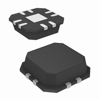
IC MOSFET DRVR SYNC BUCK 8-QFN
Manufacturer
Intersil
Datasheet
1.ISL6208ACBZ.pdf
(10 pages)
Specifications of ISL6208ACRZ
Configuration
High and Low Side, Synchronous
Input Type
PWM
Delay Time
26ns
Current - Peak
2A
Number Of Configurations
1
Number Of Outputs
2
High Side Voltage - Max (bootstrap)
33V
Voltage - Supply
4.5 V ~ 5.5 V
Operating Temperature
-10°C ~ 100°C
Mounting Type
Surface Mount
Package / Case
8-VQFN
Lead Free Status / RoHS Status
Lead free / RoHS Compliant


Functional Pin Description
UGATE (Pin 1 for SOIC-8, Pin 8 for QFN)
The UGATE pin is the upper gate drive output. Connect to
the gate of high-side power N-Channel MOSFET.
BOOT (Pin 2 for SOIC-8, Pin 1 for QFN)
BOOT is the floating bootstrap supply pin for the upper gate
drive. Connect the bootstrap capacitor between this pin and
the PHASE pin. The bootstrap capacitor provides the charge
to turn on the upper MOSFET. See the Bootstrap Diode and
Capacitor section under DESCRIPTION for guidance in
choosing the appropriate capacitor value.
PWM (Pin 3 for SOIC-8, Pin 2 for QFN)
The PWM signal is the control input for the driver. The PWM
signal can enter three distinct states during operation (see
the three-state PWM Input section under DESCRIPTION for
further details). Connect this pin to the PWM output of the
controller.
GND (Pin 4 for SOIC-8, Pin 3 for QFN)
GND is the ground pin for the IC.
LGATE (Pin 5 for SOIC-8, Pin 4 for QFN)
LGATE is the lower gate drive output. Connect to gate of the
low-side power N-Channel MOSFET.
VCC (Pin 6 for SOIC-8, Pin 5 for QFN)
Connect the VCC pin to a +5V bias supply. Place a high
quality bypass capacitor from this pin to GND.
FCCM (Pin 7 for SOIC-8, Pin 6 for QFN)
The FCCM pin enables or disables Diode Emulation. When
FCCM is LOW, diode emulation is allowed. Otherwise,
continuous conduction mode is forced. See the Diode
Emulation section under DESCRIPTION for more detail.
This pin can also be used to program additional switching
dead-time by placing a resistor in series with the input. See
the Programmable Dead-Time section for more detail.
5
ISL6208A
PHASE (Pin 8 for SOIC-8, Pin 7 for QFN)
Connect the PHASE pin to the source of the upper MOSFET
and the drain of the lower MOSFET. This pin provides a
return path for the upper gate driver.
Description
Theory of Operation
Designed for speed, the ISL6208A dual MOSFET driver
controls both high-side and low-side N-Channel FETs from
one externally provided PWM signal.
A rising edge on PWM initiates the turn-off of the lower
MOSFET (see Timing Diagram). After a short propagation
delay [t
[t
Adaptive shoot-through circuitry monitors the LGATE
voltage. When LGATE has fallen below 1V, UGATE is
allowed to turn ON. This prevents both the lower and upper
MOSFETs from conducting simultaneously, or shoot-
through.
A falling transition on PWM indicates the turn-off of the upper
MOSFET and the turn-on of the lower MOSFET. A short
propagation delay [t
gate begins to fall [t
voltage is monitored, and the lower gate is allowed to rise
after the upper MOSFET gate-to-source voltage drops below
1V. The lower gate then rises [t
MOSFET.
This driver is optimized for converters with large step down
compared to the upper MOSFET because the lower
MOSFET conducts for a much longer time in a switching
period. The lower gate driver is therefore sized much larger
to meet this application requirement.
The 0.5Ω on-resistance and 4A sink current capability
enable the lower gate driver to absorb the current injected to
the lower gate through the drain-to-gate capacitor of the
lower MOSFET and prevent a shoot through caused by the
high dv/dt of the phase node.
FL
] are provided in the Electrical Specifications section.
PDLL
], the lower gate begins to fall. Typical fall times
FU
PDLU
]. The upper MOSFET gate-to-source
] is encountered before the upper
RL
], turning on the lower
February 15, 2006
FN9272.0
Related parts for ISL6208ACRZ
Image
Part Number
Description
Manufacturer
Datasheet
Request
R

Part Number:
Description:
High Voltage Synchronous Rectified Buck MOSFET Driver
Manufacturer:
Intersil Corporation
Datasheet:
Part Number:
Description:
Intersil Corporation [CMOS Serial Controller Interface]
Manufacturer:
Intersil Corporation
Datasheet:
Part Number:
Description:
Manufacturer:
Intersil Corporation
Datasheet:
Part Number:
Description:
357-036-542-201 CARDEDGE 36POS DL .156 BLK LOPRO
Manufacturer:
Intersil Corporation
Datasheet:
Part Number:
Description:
1024-Word x 4-Bit LSI Static RAM
Manufacturer:
Intersil Corporation
Datasheet:
Part Number:
Description:
General Purpose NPN Transistor Arrays FN341.4
Manufacturer:
Intersil Corporation
Datasheet:
Part Number:
Description:
CMOS 16-Bit Microprocessor
Manufacturer:
Intersil Corporation
Datasheet:
Part Number:
Description:
Manufacturer:
Intersil Corporation
Datasheet:
Part Number:
Description:
Manufacturer:
Intersil Corporation
Datasheet:
Part Number:
Description:
Manufacturer:
Intersil Corporation
Datasheet:
Part Number:
Description:
Manufacturer:
Intersil Corporation
Datasheet:
Part Number:
Description:
CMOS 6-Bit Latch and Decoder Memory Interfaces
Manufacturer:
Intersil Corporation
Datasheet:
Part Number:
Description:
CA3046General Purpose NPN Transistor Arrays
Manufacturer:
Intersil Corporation
Datasheet:
Part Number:
Description:
Manufacturer:
Intersil Corporation
Datasheet:
Part Number:
Description:
TR909 DLC/FLC SLIC with Low Power Standby
Manufacturer:
Intersil Corporation
Datasheet: