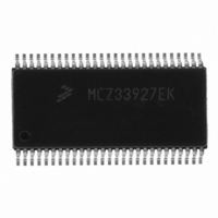
MCZ33927EK Freescale Semiconductor, MCZ33927EK Datasheet - Page 13

MCZ33927EK
Manufacturer Part Number
MCZ33927EK
Description
IC FET PRE-DRIVER 3PH 54-SOIC
Manufacturer
Freescale Semiconductor
Specifications of MCZ33927EK
Configuration
3 Phase Bridge
Input Type
Inverting and Non-Inverting
Delay Time
265ns
Current - Peak
600mA
Number Of Configurations
1
Number Of Outputs
3
High Side Voltage - Max (bootstrap)
75V
Voltage - Supply
8 V ~ 40 V
Operating Temperature
-40°C ~ 125°C
Mounting Type
Surface Mount
Package / Case
54-SOIC (7.5mm Width) Exposed Pad, 54-eSOIC, 54-HSOIC
Lead Free Status / RoHS Status
Lead free / RoHS Compliant
Available stocks
Company
Part Number
Manufacturer
Quantity
Price
Table 4. Dynamic Electrical Characteristics
values noted reflect the approximate parameter means at T
Analog Integrated Circuit Device Data
Freescale Semiconductor
INTERNAL REGULATORS
CHARGE PUMP
GATE DRIVE
Notes
V
VLS Power-Up Time
Charge Pump Oscillator Frequency
Charge Pump Slew Rate
High-Side Turn-On Time
High-Side Turn-On Delay
High-Side Turn-Off Time
High-Side Turn-Off Delay
Low-Side Turn-On Time
Low-Side Turn-On Delay
Low-Side Turn-Off Time
Low-Side Turn-Off Delay
Same Phase Command Delay Match
Thermal Filter Duration
32.
33.
34.
35.
36.
37.
Characteristics noted under conditions 8.0V ≤ V
DD
8.0V ≤ V
16V ≤ V
Transition Time from 1.0 to 10V, Load: C = 500pF, Rg = 0,
Delay from Command to 1.0V,
Transition Time from 10 to 1.0V, Load: C = 500pF, Rg = 0,
Delay from Command to 10V,
Transition Time from 1.0 to 10V, Load: C = 500pF, Rg = 0,
Delay from Command to 1.0V,
Transition Time from 10 to 1.0V, Load: C = 500pF, Rg = 0,
Delay from Command to 10V,
Power-Up Time (Until INT High)
The power-up time of the IC depends in part on the time required for this regulator to charge up the external filter capacitor on V
The power-up time of the IC depends in part on the time required for this regulator to charge up the external filter capacitor on VLS. This
delay includes the expected time for V
The charge pump operating at 12V V
These delays include all logic delays except deadtime. All internal logic is synchronous with the internal clock. The total delay includes
one clock period for state machine decision block, an additional clock period for FULLON mux logic, input synchronization time and
output driver propagation delay. Subtract one clock period for operation in FULLON mode which bypasses the state machine decision
block. Synchronization time accounts for up to one clock period of variation. See
This is the maximum separation or overlap of the High and Low side gate drives due to propagation delays when commanding one ON
and the other OFF simultaneously.
The output of the overtemperature comparator goes through a digital filter before generating a warning or interrupt.
PWR
PWR
(33)
(32)
(37)
(34)
(35)
(35)
(35)
(35)
Characteristic
(Figure
(Figure
(Figure
(Figure
(36)
DYNAMIC ELECTRICAL CHARACTERISTICS
8)
8)
7)
7)
bat
DD
, 1µF pump capacitor, MUR120 diodes and 47µF filter capacitor.
to rise.
PWR
= V
(Figure
(Figure
(Figure
(Figure
BAT
A
= 25°C under nominal conditions unless otherwise noted.
≤ 40V, -40°C ≤ T
7)
8)
7)
8)
Symbol
t
t
t
t
t
t
PU_VDD
PU_VDD
D_OFFH
t
D_OFFL
SR
D_ONH
D_DIFF
F
t
D_ONL
t
t
t
OFFH
t
OFFL
ONH
ONL
DUR
OSC
CP
Figure
A
≤ 125°C, unless otherwise noted. Typical
DYNAMIC ELECTRICAL CHARACTERISTICS
6.
Min
130
130
130
130
-20
8.0
90
–
–
–
–
–
–
–
ELECTRICAL CHARACTERISTICS
Typ
125
100
265
265
265
265
20
20
20
20
–
–
0
–
Max
+20
190
386
386
386
386
2.0
2.0
35
35
35
35
30
–
Unit
V/µs
kHz
ms
ms
ns
ns
ns
ns
ns
ns
ns
ns
ns
µs
DD
33927
.
13


