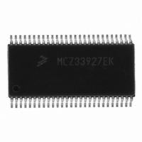
MCZ33927EK Freescale Semiconductor, MCZ33927EK Datasheet - Page 24

MCZ33927EK
Manufacturer Part Number
MCZ33927EK
Description
IC FET PRE-DRIVER 3PH 54-SOIC
Manufacturer
Freescale Semiconductor
Specifications of MCZ33927EK
Configuration
3 Phase Bridge
Input Type
Inverting and Non-Inverting
Delay Time
265ns
Current - Peak
600mA
Number Of Configurations
1
Number Of Outputs
3
High Side Voltage - Max (bootstrap)
75V
Voltage - Supply
8 V ~ 40 V
Operating Temperature
-40°C ~ 125°C
Mounting Type
Surface Mount
Package / Case
54-SOIC (7.5mm Width) Exposed Pad, 54-eSOIC, 54-HSOIC
Lead Free Status / RoHS Status
Lead free / RoHS Compliant
Available stocks
Company
Part Number
Manufacturer
Quantity
Price
five major functional blocks:
• Logic Inputs and Interface
• Bootstrap Supply
• Low-Side Drivers
• High-Side Drivers
• Charge Pump
LOGIC INPUTS AND INTERFACE
through timers.
hysteresis. Logic inputs are 3V compatible. The logic outputs
are driven from the internal supply of approximately 5.0V.
When the internal supply is not enabled, the SO pin should
not be externally driven high.
in the LOGIC COMMANDS AND REGISTERS section of this
document. SPI functionality includes the following:
• Programming of deadtime delay —This delay is
• Enabling of simultaneous operation of high-side and
• Setting of various operating modes of the IC and
24
33927
FUNCTIONAL INTERNAL BLOCK DESCRIPTION
INTRODUCTION
All functions of the IC can be described as the following
This section contains the SPI port, control logic, and shoot-
The IC logic inputs have Schmitt trigger inputs with
The SPI registers and functionality is described completely
adjustable in approximately 50 ns steps from 0 ns to
12 µs. Calibration of the delay, because of internal IC
variations, is performed via the SPI.
low-side FETs —Normally, both FETs would not be
enabled simultaneously. However, for certain applications
where the load is connected between the high-side and
low-side FETs, this could be advantageous. If this mode is
enabled, the blanking time delay will be disabled. A
sequence of commands may be required to enable this
function to prevent inadvertent enabling. In addition, this
command can only be executed once after reset to enable
or disable simultaneous turn-on.
enabling of interrupt sources.
The 33927 allows different operating modes to be set and
FUNCTIONAL INTERNAL BLOCK DESCRIPTION
Figure 10. Functional Internal Block Description
AND INTERFACE
LOGIC INPUTS
LOW-SIDE
DRIVERS
CHARGE
PUMP
• Read back of internal registers .
This means the leading edge on an input will cause the
complementary output to immediately turn off and the
selected one to turn on after the deadtime delay as illustrated
in
corresponding FET was commanded off (see
Figure
BOOTSTRAP SUPPLY (VPWR)
the bootstrap capacitors. It also supplies the peak currents
required for the low-side gate drivers.
the VPWR pin. This pin can be connected to VBAT and is
capable of withstanding up to the full load dump voltage of the
system. However, the IC only requires a low-voltage supply
Figure
locked by a SPI command (FULLON, Desaturation Fault,
Zero-Deadtime). SPI commands can also determine how
the various faults are (or are not) reported.
The status of the 33927 Status Registers can be read back
by the Master (DSP or MCU).
The Px_HS and Px_LS logic inputs are edge sensitive.
This is the portion of the IC providing current to recharge
The power for the gate drive circuits is provided through
Figure 11. Edge Sensitive Logic Inputs (Phase A)
BOOTSTRAP
PA _HS
PA_LS
PA_HS_G
PA_LS_G
HIGH-SIDE
DRIVERS
SUPPLY
11).
11. The deadtime delay timer starts when the
Analog Integrated Circuit Device Data
De adt ime
De lay
Freescale Semiconductor
Figure 6
and


