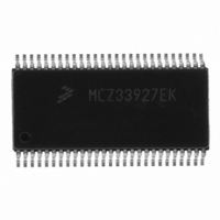
MCZ33927EK Freescale Semiconductor, MCZ33927EK Datasheet - Page 8

MCZ33927EK
Manufacturer Part Number
MCZ33927EK
Description
IC FET PRE-DRIVER 3PH 54-SOIC
Manufacturer
Freescale Semiconductor
Specifications of MCZ33927EK
Configuration
3 Phase Bridge
Input Type
Inverting and Non-Inverting
Delay Time
265ns
Current - Peak
600mA
Number Of Configurations
1
Number Of Outputs
3
High Side Voltage - Max (bootstrap)
75V
Voltage - Supply
8 V ~ 40 V
Operating Temperature
-40°C ~ 125°C
Mounting Type
Surface Mount
Package / Case
54-SOIC (7.5mm Width) Exposed Pad, 54-eSOIC, 54-HSOIC
Lead Free Status / RoHS Status
Lead free / RoHS Compliant
Available stocks
Company
Part Number
Manufacturer
Quantity
Price
Table 3. Static Electrical Characteristics
values noted reflect the approximate parameter means at T
8
33927
ELECTRICAL CHARACTERISTICS
STATIC ELECTRICAL CHARACTERISTICS
POWER INPUTS
VDD V INTERNAL REGULATOR
VLS REGULATOR
Notes
VBAT Supply Voltage Startup Threshold
VBAT Supply Current, V
VPWR Supply Current, V
Sleep State Supply Current, RST = 0V
Sleep State Output Gate Voltage
Trickle Charge Pump (Bootstrap Voltage)
Bootstrap Diode Forward Voltage at 10mA
V
Internal V
Peak Output Current, V
Linear Regulator Output Voltage, I
VLS Disable Threshold
10.
11.
12.
Characteristics noted under conditions 8.0V ≤ V
DD
8.
9.
RST and ENABLE = 5.0V
No output loads on Gate Drive Pins, No PWM
No output loads on Gate Drive Pins, 20kHz, 50% Duty Cycle
RST and ENABLE = 5.0V
No output loads on Gate Drive Pins, No PWM
Output Loads = 620nC per FET, 20kHz PWM
V
V
IG < 100µA
V
External Load I
BAT
PWR
BAT
Output Voltage, V
When minimum system voltage could be less than 14V operation with the Charge Pump is recommended. V
threshold in order for the Charge Pump and V
will continue to operate even if V
This parameter is guaranteed by design. It is not production tested.
Minimum external capacitor for stable V
Recommended external capacitor for the V
When V
= 40V
= 14V
= 40V
DD
Supply Current, V
LS
is less than this value, the outputs are disabled and HOLDOFF circuits are active.
DD_EXT
PWR
(12)
PWR
PWR
PWR
= 0 to 1.0mA
= 8V to 40V, C = 0.47µF
Characteristic
= 16V, V
= V
= V
DD
BAT
BAT
= 5.5V, No External Load
VLS
= 40V
LS
= 40V
= 0 to 60mA
BAT
= 10V
(8)
STATIC ELECTRICAL CHARACTERISTICS
drops below 6.0V.
DD
(9)
operation is 0.47µF.
LS
(11)
(10)
DD
regulator is 2.2µF low ESR at each pin VLS and VLS_CAP.
PWR
regulator to startup and drive V
= V
BAT
A
= 25°C under nominal conditions unless otherwise noted.
≤ 40V, -40°C ≤ T
V
I
Symbol
V
V
PWR_ON
GATESS
BAT_ST
V
I
I
PEAK
THVLS
I
I
V
PWR
V
I
BAT
BAT
V
Boot
DD
DD
LS
F
PWR
A
≤ 125°C, unless otherwise noted. Typical
to > 8.0V. Once V
13.5
Min
350
4.5
7.5
22
–
–
–
–
–
–
–
–
–
–
Analog Integrated Circuit Device Data
Typ
600
6.0
1.0
8.0
11
14
56
28
15
–
–
–
–
–
–
PWR
Freescale Semiconductor
exceeds 8.0V, the circuits
BAT
must exceed this
Max
100
800
8.0
1.3
1.2
5.5
8.5
10
20
95
30
32
12
17
–
Unit
mA
mA
mA
mA
µA
V
V
V
V
V
V
V


