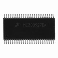
MCZ33927EK Freescale Semiconductor, MCZ33927EK Datasheet - Page 32

MCZ33927EK
Manufacturer Part Number
MCZ33927EK
Description
IC FET PRE-DRIVER 3PH 54-SOIC
Manufacturer
Freescale Semiconductor
Specifications of MCZ33927EK
Configuration
3 Phase Bridge
Input Type
Inverting and Non-Inverting
Delay Time
265ns
Current - Peak
600mA
Number Of Configurations
1
Number Of Outputs
3
High Side Voltage - Max (bootstrap)
75V
Voltage - Supply
8 V ~ 40 V
Operating Temperature
-40°C ~ 125°C
Mounting Type
Surface Mount
Package / Case
54-SOIC (7.5mm Width) Exposed Pad, 54-eSOIC, 54-HSOIC
Lead Free Status / RoHS Status
Lead free / RoHS Compliant
Available stocks
Company
Part Number
Manufacturer
Quantity
Price
DEADTIME COMMAND
same phase until the deadtime has expired. The deadtime
timer starts when a FET is commanded off (see
Figure
FULLON mode.
(100x xxx1), and then sending a calibration pulse of CS. This
pulse must be 16 times longer than the required deadtime
(see
internal time base,
and stored in an internal register to provide the reference for
timing the deadtime between high and low gate transactions
in the same phase.
and a 1.5 µs deadtime is required. First a DEADTIME
command is sent (using the SPI), then a CS is sent. The CS
pulse is 16*1.5=24 µs wide. The IC measures this pulse as
24000ns/50ns = 480 clock cycles and stores 480/16=30 in
the deadtime register. Until the next deadtime calibration is
32
Table 13. .DEADTIME Command
33927
FUNCTIONAL DEVICE OPERATION
LOGIC COMMANDS AND REGISTERS
SPI Data Bits
Write
Reset
Deadtime prevents the turn-on of both transistors in the
The deadtime is set by sending the DEADTIME command
For example: the internal time base is running at 20MHz
Figure
11). The deadtime control is disabled by enabling the
CS
SO
SI
SCLK
16). Deadtime is measured in cycle times of the
f
TB
. This measurement is divided by 16
7
1
6
0
DEADTIME
Command
Figure 16. Deadtime Calibration
Figure 6
5
0
and
4
x
performed, 30 clock cycles will separate the turn off and turn
on gate signals in the same phase. The worst case error
immediately after calibration will be +0/-1 time base cycle, for
this example +0ns/-50ns. Note that if the internal time base
drifts, the effect on dead time will scale directly.
the deadtime timer to 0. However, simultaneous turn-on of
high-side and low-side FETs in the same phase is still
prevented unless the FULLON command has been
transmitted. There is no calibration pulse expected after
receiving the ZERO DEADTIME command.
time base cycles (typically 15 µs).
calibration pulse. If there are any transitions on SI or SCLK
while the Deadtime CS pulse is low, a Framing Error will be
generated, however, the CS pulse will be used to calibrate
the deadtime
Sending a ZERO DEADTIME command (100x xxx0) sets
After RESET, deadtime is set to the maximum value of 255
The IC ignores any SPI data that is sent during the
Deadtime Calibration Pulse
3
x
x
Analog Integrated Circuit Device Data
2
x
x
Freescale Semiconductor
1
x
x
CALIBRATE
ZERO/
0
x


