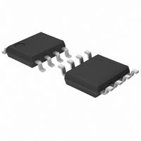
BD6519FJ-E2 Rohm Semiconductor, BD6519FJ-E2 Datasheet - Page 16

BD6519FJ-E2
Manufacturer Part Number
BD6519FJ-E2
Description
IC SWITCH HIGH SIDE 1CH SOP-J8
Manufacturer
Rohm Semiconductor
Type
High Sider
Specifications of BD6519FJ-E2
Input Type
Non-Inverting
Number Of Outputs
1
On-state Resistance
100 mOhm
Current - Output / Channel
500mA
Current - Peak Output
1A
Voltage - Supply
3 V ~ 5.5 V
Operating Temperature
-40°C ~ 85°C
Mounting Type
Surface Mount
Package / Case
8-SOPJ
Primary Input Voltage
5V
No. Of Outputs
1
Output Voltage
5V
Output Current
500mA
Voltage Regulator Case Style
SOP
No. Of Pins
8
Operating Temperature Range
-40°C To +85°C
Svhc
No SVHC
Output Power
560 mW
Input Voltage
3 V to 5.5 V
Mounting Style
SMD/SMT
Lead Free Status / RoHS Status
Lead free / RoHS Compliant
Lead Free Status / RoHS Status
Lead free / RoHS Compliant, Lead free / RoHS Compliant
Other names
BD6519FJ-E2TR
Available stocks
Company
Part Number
Manufacturer
Quantity
Price
Part Number:
BD6519FJ-E2
Manufacturer:
ROHM/罗姆
Quantity:
20 000
Application information
Power dissipation character
Notes for use
© 2009 ROHM Co., Ltd. All rights reserved.
BD2041AFJ,BD2051AFJ,BD6518FJ,BD6519FJ
www.rohm.com
(1) Absolute Maximum Ratings
(2) Operating conditions
(3) Reverse connection of power supply connector
When excessive current flows owing to output shortcircuit or so, ringing occurs by inductance of power source line to IC, and
may cause bad influences upon IC actions. In order to avoid this case, connect a bypath capacitor by IN terminal and GND
terminal of IC. 1μF or higher is recommended.
Pull up /OC output by resistance 10kΩ ~ 100kΩ.
Set up value which satisfies the application as C
This system connection diagram doesn’t guarantee operating as the application.
The external circuit constant and so on is changed and it uses, in which there are adequate margins by taking into account
external parts or dispersion of IC including not only static characteristics but also transient characteristics.
(SOP-J8)
※
An excess in the absolute maximum ratings, such as supply voltage, temperature range of operating conditions, etc., can
break down devices, thus making impossible to identify breaking mode such as a short circuit or an open circuit. If any
special mode exceeding the absolute maximum ratings is assumed, consideration should be given to take physical safety
measures including the use of fuses, etc.
These conditions represent a range within which characteristics can be provided approximately as expected.
The electrical characteristics are guaranteed under the conditions of each parameter.
The reverse connection of power supply connector can break down ICs. Take protective measures against the breakdown
due to the reverse connection, such as mounting an external diode between the power supply and the IC’s power supply
terminal.
IN, EN (/EN), and /OC terminal of BD2041AFJ/BD2051AFJ correspond to VDD, CTRL, and FLAG terminal of BD6518FJ/BD6519FJ, respectively.
600
500
400
300
200
100
0
0
25
Fig.77 Power dissipation curve (Pd-Ta Curve)
AMBIENT TEMPERATURE: Ta [ ℃ ]
L
50
and Ferrite Beads.
16/18
75
100
125
150
Technical Note
2009.05 - Rev.A


