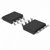
BD6519FJ-E2 Rohm Semiconductor, BD6519FJ-E2 Datasheet - Page 17

BD6519FJ-E2
Manufacturer Part Number
BD6519FJ-E2
Description
IC SWITCH HIGH SIDE 1CH SOP-J8
Manufacturer
Rohm Semiconductor
Type
High Sider
Specifications of BD6519FJ-E2
Input Type
Non-Inverting
Number Of Outputs
1
On-state Resistance
100 mOhm
Current - Output / Channel
500mA
Current - Peak Output
1A
Voltage - Supply
3 V ~ 5.5 V
Operating Temperature
-40°C ~ 85°C
Mounting Type
Surface Mount
Package / Case
8-SOPJ
Primary Input Voltage
5V
No. Of Outputs
1
Output Voltage
5V
Output Current
500mA
Voltage Regulator Case Style
SOP
No. Of Pins
8
Operating Temperature Range
-40°C To +85°C
Svhc
No SVHC
Output Power
560 mW
Input Voltage
3 V to 5.5 V
Mounting Style
SMD/SMT
Lead Free Status / RoHS Status
Lead free / RoHS Compliant
Lead Free Status / RoHS Status
Lead free / RoHS Compliant, Lead free / RoHS Compliant
Other names
BD6519FJ-E2TR
Available stocks
Company
Part Number
Manufacturer
Quantity
Price
Part Number:
BD6519FJ-E2
Manufacturer:
ROHM/罗姆
Quantity:
20 000
© 2009 ROHM Co., Ltd. All rights reserved.
BD2041AFJ,BD2051AFJ,BD6518FJ,BD6519FJ
www.rohm.com
(10) Ground wiring pattern
(11) External capacitor
(12) Thermal shutdown circuit (TSD)
(13) Thermal design
(4) Power supply line
(5) GND voltage
(6) Short circuit between terminals and erroneous mounting
(7) Operation in strong electromagnetic field
(8) Inspection with set PCB
(9) Input terminals
Design PCB pattern to provide low impedance for the wiring between the power supply and the GND lines. In this regard,
for the digital block power supply and the analog block power supply, even though these power supplies has the same
level of potential, separate the power supply pattern for the digital block from that for the analog block, thus suppressing
the diffraction of digital noises to the analog block power supply resulting from impedance common to the wiring patterns.
For the GND line, give consideration to design the patterns in a similar manner.
Furthermore, for all power supply terminals to ICs, mount a capacitor between the power supply and the GND terminal. At
the same time, in order to use an electrolytic capacitor, thoroughly check to be sure the characteristics of the capacitor to
be used present no problem including the occurrence of capacity dropout at a low temperature, thus determining the
constant.
Make setting of the potential of the GND terminal so that it will be maintained at the minimum in any operating state.
Furthermore, check to be sure no terminals are at a potential lower than the GND voltage including an actual electric
transient.
In order to mount ICs on a set PCB, pay thorough attention to the direction and offset of the ICs. Erroneous mounting can
break down the ICs. Furthermore, if a short circuit occurs due to foreign matters entering between terminals or between
the terminal and the power supply or the GND terminal, the ICs can break down.
Be noted that using ICs in the strong electromagnetic field can malfunction them.
On the inspection with the set PCB, if a capacitor is connected to a low-impedance IC terminal, the IC can suffer stress.
Therefore, be sure to discharge from the set PCB by each process. Furthermore, in order to mount or dismount the set
PCB to/from the jig for the inspection process, be sure to turn OFF the power supply and then mount the set PCB to the jig.
After the completion of the inspection, be sure to turn OFF the power supply and then dismount it from the jig. In addition,
for protection against static electricity, establish a ground for the assembly process and pay thorough attention to the
transportation and the storage of the set PCB.
In terms of the construction of IC, parasitic elements are inevitably formed in relation to potential. The operation of the
parasitic element can cause interference with circuit operation, thus resulting in a malfunction and then breakdown of the
input terminal. Therefore, pay thorough attention not to handle the input terminals, such as to apply to the input terminals a
voltage lower than the GND respectively, so that any parasitic element will operate. Furthermore, do not apply a voltage to
the input terminals when no power supply voltage is applied to the IC. In addition, even if the power supply voltage is
applied, apply to the input terminals a voltage lower than the power supply voltage or within the guaranteed value of
electrical characteristics.
If small-signal GND and large-current GND are provided, It will be recommended to separate the large-current GND
pattern from the small-signal GND pattern and establish a single ground at the reference point of the set PCB so that
resistance to the wiring pattern and voltage fluctuations due to a large current will cause no fluctuations in voltages of the
small-signal GND. Pay attention not to cause fluctuations in the GND wiring pattern of external parts as well.
In order to use a ceramic capacitor as the external capacitor, determine the constant with consideration given to a
degradation in the nominal capacitance due to DC bias and changes in the capacitance due to temperature, etc.
When junction temperatures become detected temperatures or higher, the thermal shutdown circuit operates and turns a
switch OFF. The thermal shutdown circuit, which is aimed at isolating the LSI from thermal runaway as much as possible,
is not aimed at the protection or guarantee of the LSI. Therefore, do not continuously use the LSI with this circuit
operating or use the LSI assuming its operation.
Perform thermal design in which there are adequate margins by taking into account the power dissipation (Pd) in actual
states of use.
17/18
Technical Note
2009.05 - Rev.A


