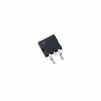
VNB35NV04 STMicroelectronics, VNB35NV04 Datasheet - Page 4

VNB35NV04
Manufacturer Part Number
VNB35NV04
Description
MOSFET N-CH 40V 30A D2PAK
Manufacturer
STMicroelectronics
Series
OMNIFET II™r
Type
Low Sider
Datasheet
1.VNB35NV04.pdf
(19 pages)
Specifications of VNB35NV04
Input Type
Non-Inverting
Number Of Outputs
1
On-state Resistance
13 mOhm
Current - Peak Output
45A
Mounting Type
Surface Mount
Package / Case
D²Pak, TO-263 (2 leads + tab)
Switch Type
Low Side
Power Switch Family
VNB35NV04
Power Switch On Resistance
13mOhm
Output Current
30A
Supply Current
100uA
Package Type
D2PAK
Mounting
Surface Mount
Power Dissipation
125W
Lead Free Status / RoHS Status
Contains lead / RoHS non-compliant
Voltage - Supply
-
Operating Temperature
-
Current - Output / Channel
-
Lead Free Status / Rohs Status
Not Compliant
Other names
497-2671-5
Available stocks
Company
Part Number
Manufacturer
Quantity
Price
Company:
Part Number:
VNB35NV04
Manufacturer:
ST
Quantity:
12 500
Part Number:
VNB35NV04
Manufacturer:
ST
Quantity:
20 000
Company:
Part Number:
VNB35NV0413TR
Manufacturer:
ST
Quantity:
12 500
Company:
Part Number:
VNB35NV04TR-E
Manufacturer:
STMicroelectronics
Quantity:
10
Part Number:
VNB35NV04TR-E
Manufacturer:
ST
Quantity:
20 000
VNB35NV04 / VNP35NV04 / VNV35NV04 / VNW35NV04
ELECTRICAL CHARACTERISTICS (continued) (T
DYNAMIC
SWITCHING
SOURCE DRAIN DIODE
PROTECTIONS (-40°C < T
(*) Pulsed: Pulse duration = 300 s, duty cycle 1.5%
4/19
2
Symbol
Symbol
Symbol
Symbol
(di/dt)
V
g
C
t
t
t
t
I
SD
t
T
d(on)
d(off)
d(on)
d(off)
RRM
E
fs
T
Q
I
dlim
OSS
Q
I
t
lim
t
t
t
t
jsh
gf
rr
jrs
as
r
r
f
f
rr
(*)
i
(*)
on
Forward
Transconductance
Output Capacitance
Turn-on Delay Time
Rise Time
Turn-off Delay Time
Fall Time
Turn-on Delay Time
Rise Time
Turn-off Delay Time
Fall Time
Turn-on Current Slope
Total Input Charge
Forward On Voltage
Reverse Recovery Time
Reverse Recovery Charge
Reverse Recovery Current
Drain Current Limit
Step Response Current
Limit
Overtemperature
Shutdown
Overtemperature Reset
Fault Sink Current
Single Pulse
Avalanche Energy
Parameter
Parameter
Parameter
Parameter
j
< 150°C, unless otherwise specified)
V
V
V
V
(see figure 1)
V
V
(see figure 1)
V
V
V
I
I
I
V
(see test circuit, figure 2)
V
V
V
starting T
V
(see figures 3 & 4)
gen
SD
SD
DD
DS
DD
gen
DD
gen
DD
gen
DD
DD
IN
IN
IN
IN
=15A; V
=15A; dI/dt=100A/ s
=6V; V
=6V; V
=5V; V
=5V; R
=13V; f=1MHz; V
=13V; I
=15V; I
=15V; I
=15V; I
=12V; I
=2.13mA (see figure 5)
=30V; L=200 H
=5V; R
=5V; R
=5V; R
j
=25°C; V
DS
DS
DS
gen
Test Conditions
D
Test Conditions
Test Conditions
Test Conditions
D
D
D
D
gen
gen
gen
IN
=15A
=15A
=15A
=15A
=15A; V
=13V
=13V
=13V; T
=0V
=R
=R
=2.2K
=R
IN MIN
j
IN MIN
IN MIN
=25°C, unless otherwise specified)
DD
IN
j
IN
=T
=24V
=4.7
=5V
=0V
=4.7
=4.7
jsh
L=24mH
Min
Min
Min
150
135
Min
1.7
30
10
1300
Typ
Typ
Typ
840
400
175
150
980
600
118
Typ
0.8
1.4
27
34
31
18
45
50
15
35
7
4
2500
3000
1500
Max
Max
Max
Max
500
100
120
110
200
60
20
12
A/ s
Unit
Unit
Unit
Unit
mA
nC
ns
°C
°C
pF
ns
ns
ns
ns
V
A
A
S
J
C
s
s
s
s
s


