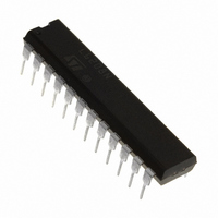
L6208N STMicroelectronics, L6208N Datasheet - Page 9

L6208N
Manufacturer Part Number
L6208N
Description
IC DRIVER STEPPER MOTOR 24PWRDIP
Manufacturer
STMicroelectronics
Type
Driverr
Datasheet
1.L6208D013TR.pdf
(27 pages)
Specifications of L6208N
Applications
Stepper Motor Driver, 2 Phase
Number Of Outputs
2
Current - Output
5.6A
Voltage - Supply
8 V ~ 52 V
Operating Temperature
-25°C ~ 125°C
Mounting Type
Through Hole
Package / Case
24-DIP (0.300", 7.62mm)
Operating Supply Voltage
8 V to 52 V
Supply Current
0.01 A
Mounting Style
Through Hole
Motor Type
Stepper
No. Of Outputs
4
Output Current
7.1A
Output Voltage
52V
Supply Voltage Range
8V To 52V
Driver Case Style
DIP
No. Of Pins
24
Rohs Compliant
Yes
For Use With
497-5488 - EVAL BOARD FOR L6208N DIP497-4136 - EVAL BOARD FOR L6208 SERIES
Lead Free Status / RoHS Status
Lead free / RoHS Compliant
Voltage - Load
-
Lead Free Status / Rohs Status
Lead free / RoHS Compliant
Other names
497-5342-5
L6208N
L6208N
Available stocks
Company
Part Number
Manufacturer
Quantity
Price
Company:
Part Number:
L6208N
Manufacturer:
STMicroelectronics
Quantity:
226
Company:
Part Number:
L6208N
Manufacturer:
POWEREX
Quantity:
1 000
Part Number:
L6208N
Manufacturer:
ST
Quantity:
20 000
Figure 5. Overcurrent Detection Timing Definition
CIRCUIT DESCRIPTION
POWER STAGES and CHARGE PUMP
The L6208 integrates two independent Power MOS Full Bridges. Each Power MOS has an R
ical value @ 25°C), with intrinsic fast freewheeling diode. Switching patterns are generated by the PWM Current
Controller and the Phase Sequence Generator (see below). Cross conduction protection is achieved using a
dead time (t
a bridge.
Pins VS
voltage in the range from 8V to 52V. It has to be noticed that the R
supply voltage is in the range from 8V to 12V (see Fig. 34 and 35).
Using N-Channel Power MOS for the upper transistors in the bridge requires a gate drive voltage above the
power supply voltage. The bootstrapped supply voltage V
external components to realize a charge pump circuit as shown in Figure 6. The oscillator output (VCP) is a
square wave at 600KHz (typical) with 10V amplitude. Recommended values/part numbers for the charge pump
circuit are shown in Table 1.
Table 1. Charge Pump External Components Values
C
C
R
D1
D2
BOOT
P
P
A
and VS
DT
= 1 s typical value) between the switch off and switch on of two Power MOSFETSs in one leg of
B
MUST be connected together to the supply voltage V
220nF
10nF
100
1N4148
1N4148
BRIDGE
I
SOVER
I
V
OUT
OFF
90%
10%
EN
ON
t
OCD(ON)
BOOT
t
OCD(OFF)
is obtained through an internal Oscillator and few
DS(ON)
increases of some percents when the
S
. The device operates with a supply
D02IN1399
DS(ON)
= 0.3 (typ-
L6208
9/27


