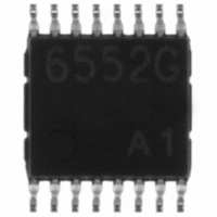
TB6552FNG(O,EL) Toshiba, TB6552FNG(O,EL) Datasheet

TB6552FNG(O,EL)
Specifications of TB6552FNG(O,EL)
TB6552FNGOEL
TB6552FNGTR
TB6552FNGTR
Related parts for TB6552FNG(O,EL)
TB6552FNG(O,EL) Summary of contents
Page 1
... Toshiba Bi-CD Integrated Circuit Silicon Monolithic TB6552FN/FNG, TB6552FL/FLG DUAL-BRIDGE DRIVER IC FOR DC MOTORS The TB6552FN/FNG/FL/FLG is a dual-bridge driver IC for DC motors with output transistors MOS structure with low ON-resistance. Two input signals, IN1 and IN2, can chose one of four modes such as CW, CCW, short brake, and stop mode. A PWM drive system supports high heat efficiency driving ...
Page 2
Block Diagram V BIN1 BIN2 CC Control logic (Ch. B) Control logic (Ch. A) GND AIN1 AIN2 Pin Functions Pin No Pin.Name FN/FNG FL/FLG GND 1 AIN1 2 AIN2 3 APWM 4 ASTBY 5 AO1 7 AO2 8 PGND 9 ...
Page 3
Input/Output Function (common for channel A and B) Input IN1 IN2 STBY H/L H/L L Operating Description • PWM control function Speed can be controlled by inputting the ...
Page 4
Switching characteristics of output transistors The switching characteristics between the PWM input and the output transistors are shown below. PWM Input (APWM, BPWM) Output Voltage (A01, A02, B01, B02) <Typical Value> Item Typical Value t 1000 pLH t 1000 ...
Page 5
Absolute Maximum Ratings Characteristics Supply voltage Input voltage Output current Power dissipation Operating temperature Storage temperature Note 1: This rating is obtained when the product is mounted × 30 × 1.6 mm glass-epoxy PCB of which 40% ...
Page 6
Electrical Characteristics Characteristics Supply current Input voltage Control circuit Hysteresis voltage Input current Input voltage Standby circuit Input current Output saturating voltage Output leakage current Diode forward voltage PWM frequency PWM control Minimum clock circuit pulse width Output transistor switching ...
Page 7
Characteristic Wave Form TB6552FN/FNG P – 1.2 (1) 50 × 30 × 1.6 mm PCB mounting occupied copper area in excess of 40% 1.0 (2) IC only θj-a = 250°C/W (1) 0.8 0.6 (2) 0.4 0 ...
Page 8
Typical Application Diagram PWM PORT1 PORT2 PORT3 PORT4 Microcontroller PWM PORT5 PORT6 PORT7 PORT8 GND Note 1: The power supply capacitor should be connected as close as possible to the IC. Note 2: When connecting the motor ...
Page 9
Requests Concerning Use of QON Outline Drawing of Package Upper surface When using QON, take into account the following items. Caution (1) Do not carry out soldering on the island sections in the four corners of the package (indicated by ...
Page 10
Package Dimensions Weight: 0.07 g (typ.) TB6552FN/FNG/FL/FLG 10 2007-4-2 ...
Page 11
Package Dimensions Weight: 0.05 g (typ.) Do not carry out soldering at the four corners of the package. 11 TB6552FN/FNG/FL/FLG 2007-4-2 ...
Page 12
... Application Circuits The application circuits shown in this document are provided for reference purposes only. Thorough evaluation is required, especially at the mass production design stage. Toshiba does not grant any license to any industrial property rights by providing these examples of application circuits. 5. Test Circuits Components in the test circuits are used only to obtain and confirm the device characteristics. These components and circuits are not guaranteed to prevent malfunction or failure from occurring in the application equipment ...
Page 13
Points to remember on handling of ICs (1) Thermal Shutdown Circuit Thermal shutdown circuits do not necessarily protect ICs under all circumstances. If the thermal shutdown circuits operate against the over temperature, clear the heat generation status immediately. Depending on ...
Page 14
... The information contained herein is presented only as a guide for the applications of our products. No responsibility is assumed by TOSHIBA for any infringements of patents or other rights of the third parties which may result from its use. No license is granted by implication or otherwise under any patents or other rights of TOSHIBA or the third parties ...


