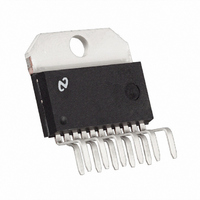
LMD18201T/NOPB National Semiconductor, LMD18201T/NOPB Datasheet

LMD18201T/NOPB
Specifications of LMD18201T/NOPB
*LMD18201T/NOPB
LMD18201T
Related parts for LMD18201T/NOPB
LMD18201T/NOPB Summary of contents
Page 1
... Low R typically 0.33Ω per switch DS(ON) Functional Diagram FIGURE 1. Functional Block Diagram of LMD18201 © 2004 National Semiconductor Corporation n TTL and CMOS compatible inputs n No “shoot-through” current n Thermal warning flag output at 145˚C n Thermal shutdown (outputs off) at 170˚C n Internal clamp diodes ...
Page 2
Connection Diagram and Ordering Information www.national.com Top View Order Number LMD18201T See NS Package Number TA11B 2 01079302 ...
Page 3
... Absolute Maximum Ratings If Military/Aerospace specified devices are required, please contact the National Semiconductor Sales Office/ Distributors for availability and specifications. Total Supply Voltage (V , Pin 6) S Voltage at Pins and 9 Voltage at Bootstrap Pins (Pins 1 and 11) Peak Output Current (200 ms) Continuous Output Current (Note 2) ...
Page 4
Typical Performance Characteristics V vs Flag Current SAT R vs DS(ON) Supply Voltage Supply Current vs Frequency (V = 42V) S www.national.com R DS(ON) 01079312 01079314 Temperature (V 01079316 4 vs Temperature 01079313 Supply Current vs Supply Voltage 01079315 Supply ...
Page 5
Test Circuit Switching Time Definitions Pinout Description (See Connection Dia- gram) Pin 1, BOOTSTRAP 1 Input: Bootstrap capacitor pin for half H-Bridge number 1. The recommended capacitor (10 nF) is connected between pins 1 and 2. Pin 2, OUTPUT 1: ...
Page 6
Application Information Sign/magnitude PWM consists of separate direction (sign) and amplitude (magnitude) signals (see Figure 3). The (ab- solute) magnitude signal is duty-cycle modulated, and the FIGURE 4. Transitions in Brake, Direction, or PWM Must be Separated by At Least ...
Page 7
Application Information below the Absolute Maximum Rating of the device. When operating the chip at supply voltages above 40V a voltage suppressor (transorb) such as P6KE62A is recommended from supply to ground. Typically the ceramic capacitor can be eliminated in ...
Page 8
Application Information reverse recovery current of 1A when tested with a full 3A of forward current through the diode. For the sinking devices the recovery time is typically 100 ns with 4A of reverse current under the same conditions. Typical ...
Page 9
Typical Applications (Continued) FIGURE 8. Current Sensing 9 01079311 www.national.com ...
Page 10
... BANNED SUBSTANCE COMPLIANCE National Semiconductor certifies that the products and packing materials meet the provisions of the Customer Products Stewardship Specification (CSP-9-111C2) and the Banned Substances and Materials of Interest Specification (CSP-9-111S2) and contain no ‘‘Banned Substances’’ as defined in CSP-9-111S2. ...


