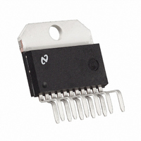
LMD18201T/NOPB National Semiconductor, LMD18201T/NOPB Datasheet - Page 7

LMD18201T/NOPB
Manufacturer Part Number
LMD18201T/NOPB
Description
IC H BRIDGE 3A 55V TO220-11
Manufacturer
National Semiconductor
Specifications of LMD18201T/NOPB
Applications
DC Motor Driver, Stepper Motor Driver, H Bridge
Number Of Outputs
1
Current - Output
3A
Voltage - Supply
12 V ~ 55 V
Operating Temperature
-40°C ~ 125°C
Mounting Type
Through Hole
Package / Case
TO-220-11 (Bent and Staggered Leads)
Lead Free Status / RoHS Status
Lead free / RoHS Compliant
Voltage - Load
-
Lead Free Status / Rohs Status
RoHS Compliant part
Electrostatic Device
Other names
*LMD18201T
*LMD18201T/NOPB
LMD18201T
*LMD18201T/NOPB
LMD18201T
Application Information
below the Absolute Maximum Rating of the device. When
operating the chip at supply voltages above 40V a voltage
suppressor (transorb) such as P6KE62A is recommended
from supply to ground. Typically the ceramic capacitor can
be eliminated in the presence of the voltage suppressor.
Note that when driving high load currents a greater amount
of supply bypass capacitance (in general at least 100 µF per
Amp of load current) is required to absorb the recirculating
currents of the inductive loads.
CURRENT LIMITING
Current limiting protection circuitry has been incorporated
into the design of the LMD18201. With any power device it is
important to consider the effects of the substantial surge
currents through the device that may occur as a result of
shorted loads. The protection circuitry monitors the current
through the upper transistors and shuts off the power device
as quickly as possible in the event of an overload condition
(the threshold is set to approximately 10A). In a typical motor
driving application the most common overload faults are
caused by shorted motor windings and locked rotors. Under
these conditions the inductance of the motor (as well as any
series inductance in the V
the magnitude of a current surge to a safe level for the
LMD18201. Once the device is shut down, the control cir-
cuitry will periodically try to turn the power device back on.
This feature allows the immediate return to normal operation
once the fault condition has been removed. While the fault
remains however, the device will cycle in and out of thermal
shutdown. This can create voltage transients on the V
supply line and therefore proper supply bypassing tech-
niques are required.
The most severe condition for any power device is a direct,
hard-wired (“screwdriver”) long term short from an output to
ground. This condition can generate a surge of current
through the power device on the order of 15 Amps and
require the die and package to dissipate up to 500W of
power for the short time required for the protection circuitry
to shut off the power device. This energy can be destructive,
particularly at higher operating voltages (
precautions are in order. Proper heat sink design is essential
and it is normally necessary to heat sink the V
(pin 6) with 1 square inch of copper on the PC board.
INTERNAL CHARGE PUMP AND USE OF
BOOTSTRAP CAPACITORS
To turn on the high-side (sourcing) DMOS power devices,
the gate of each device must be driven approximately 8V
more positive than the supply voltage. To achieve this an
internal charge pump is used to provide the gate drive volt-
age. As shown in (Figure 5), an internal capacitor is alter-
nately switched to ground and charged to about 14V, then
switched to V
than V
running internal 300 kHz oscillator. The rise time of this drive
voltage is typically 20 µs which is suitable for operating
frequencies up to 1 kHz.
S
. This switching action is controlled by a continuously
S
thereby providing a gate drive voltage greater
CC
supply line) serves to reduce
(Continued)
>
30V) so some
CC
supply pin
CC
7
For higher switching frequencies, the LMD18201 provides
for the use of external bootstrap capacitors. The bootstrap
principle is in essence a second charge pump whereby a
large value capacitor is used which has enough energy to
quickly charge the parasitic gate input capacitance of the
power device resulting in much faster rise times. The switch-
ing action is accomplished by the power switches them-
selves (Figure 6). External 10 nF capacitors, connected from
the outputs to the bootstrap pins of each high-side switch
provide typically less than 100 ns rise times allowing switch-
ing frequencies up to 500 kHz.
INTERNAL PROTECTION DIODES
A major consideration when switching current through induc-
tive loads is protection of the switching power devices from
the large voltage transients that occur. Each of the four
switches in the LMD18201 have a built-in protection diode to
clamp transient voltages exceeding the positive supply or
ground to a safe diode voltage drop across the switch.
The reverse recovery characteristics of these diodes, once
the transient has subsided, is important. These diodes must
come out of conduction quickly and the power switches must
be able to conduct the additional reverse recovery current of
the diodes. The reverse recovery time of the diodes protect-
ing the sourcing power devices is typically only 70 ns with a
FIGURE 5. Internal Charge Pump Circuitry
FIGURE 6. Bootstrap Circuitry
01079306
www.national.com
01079307


