LMD18201T/NOPB National Semiconductor, LMD18201T/NOPB Datasheet - Page 6
LMD18201T/NOPB
Manufacturer Part Number
LMD18201T/NOPB
Description
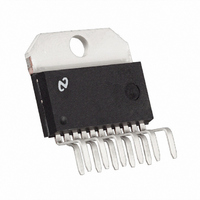
IC H BRIDGE 3A 55V TO220-11
Manufacturer
National Semiconductor
Specifications of LMD18201T/NOPB
Applications
DC Motor Driver, Stepper Motor Driver, H Bridge
Number Of Outputs
1
Current - Output
3A
Voltage - Supply
12 V ~ 55 V
Operating Temperature
-40°C ~ 125°C
Mounting Type
Through Hole
Package / Case
TO-220-11 (Bent and Staggered Leads)
Lead Free Status / RoHS Status
Lead free / RoHS Compliant
Voltage - Load
-
Lead Free Status / Rohs Status
RoHS Compliant part
Electrostatic Device
Other names
*LMD18201T
*LMD18201T/NOPB
LMD18201T
*LMD18201T/NOPB
LMD18201T


www.national.com
Application Information
Sign/magnitude PWM consists of separate direction (sign)
and amplitude (magnitude) signals (see Figure 3). The (ab-
solute) magnitude signal is duty-cycle modulated, and the
SIGNAL TRANSITION REQUIREMENTS
To ensure proper internal logic performance, it is good prac-
tice to avoid aligning the falling and rising edges of input
signals. A delay of at least 1 µsec should be incorporated
between transitions of the Direction, Brake, and/or PWM
input signals. A conservative approach is be sure there is at
least 500ns delay between the end of the first transition and
the beginning of the second transition. See Figure 4.
USING THE THERMAL WARNING FLAG
The THERMAL FLAG output (pin 9) is an open collector
transistor. This permits a wired OR connection of thermal
warning flag outputs from multiple LMD18201’s, and allows
the user to set the logic high level of the output signal swing
to match system requirements. This output typically drives
FIGURE 4. Transitions in Brake, Direction, or PWM Must be Separated by At Least 1 µsec
FIGURE 3. Sign/Magnitude PWM Control
(Continued)
6
absence of a pulse signal (a continuous logic low level)
represents zero drive. Current delivered to the load is pro-
portional to pulse width. For the LMD18201, the DIRECTION
input (pin 3) is driven by the sign signal and the PWM input
(pin 5) is driven by the magnitude signal.
the interrupt input of a system controller. The interrupt ser-
vice routine would then be designed to take appropriate
steps, such as reducing load currents or initiating an orderly
system shutdown. The maximum voltage compliance on the
flag pin is 12V.
SUPPLY BYPASSING
During switching transitions the levels of fast current
changes experienced may cause troublesome voltage tran-
sients across system stray inductances.
It is normally necessary to bypass the supply rail with a high
quality capacitor(s) connected as close as possible to the V
Power Supply (Pin 6) and POWER GROUND (Pin 7). A 1 µF
high-frequency ceramic capacitor is recommended. Care
should be taken to limit the transients on the supply pin
01079305
01079324
S
Related parts for LMD18201T/NOPB
Image
Part Number
Description
Manufacturer
Datasheet
Request
R

Part Number:
Description:
IC, MOTOR CTRL, HALF BRIDGE 3A TO-220-11
Manufacturer:
National Semiconductor
Datasheet:

Part Number:
Description:
National Semiconductor [8-Bit D/A Converter]
Manufacturer:
National Semiconductor
Datasheet:
Part Number:
Description:
National Semiconductor [Media Coprocessor]
Manufacturer:
National Semiconductor
Datasheet:
Part Number:
Description:
Digitally Controlled Tone and Volume Circuit with Stereo Audio Power Amplifier, Microphone Preamp Stage and National 3D Sound
Manufacturer:
National Semiconductor
Datasheet:
Part Number:
Description:
Digitally Controlled Tone and Volume Circuit with Stereo Audio Power Amplifier, Microphone Preamp Stage and National 3D Sound
Manufacturer:
National Semiconductor
Datasheet:
Part Number:
Description:
AC97 Rev 2 Codec with Sample Rate Conversion and National 3D Sound
Manufacturer:
National Semiconductor
Part Number:
Description:
Manufacturer:
National Semiconductor
Datasheet:
Part Number:
Description:
Manufacturer:
National Semiconductor
Datasheet:
Part Number:
Description:
General Purpose, Low Voltage, Low Power, Rail-to-Rail Output Operational Amplifiers
Manufacturer:
National Semiconductor
Datasheet:
Part Number:
Description:
8-bit 20 MSPS flash A/D converter.
Manufacturer:
National Semiconductor
Datasheet:
Part Number:
Description:
Low Noise Quad Operational Amplifier
Manufacturer:
National Semiconductor
Datasheet:
Part Number:
Description:
Quad Differential Line Receivers
Manufacturer:
National Semiconductor
Datasheet:
Part Number:
Description:
Quad High Speed Trapezoidal? Bus Transceiver
Manufacturer:
National Semiconductor
Datasheet:
Part Number:
Description:
Dual Line Receiver
Manufacturer:
National Semiconductor
Datasheet: