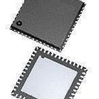
MAX16065ETM+ Maxim Integrated Products, MAX16065ETM+ Datasheet - Page 39

MAX16065ETM+
Manufacturer Part Number
MAX16065ETM+
Description
IC SYSTEM MANAGER 12CH 48-TQFN
Manufacturer
Maxim Integrated Products
Datasheet
1.MAX16065ETM.pdf
(62 pages)
Specifications of MAX16065ETM+
Applications
Power Supply Monitor, Sequencer
Voltage - Supply
2.8 V ~ 14 V
Current - Supply
4.5mA
Operating Temperature
-40°C ~ 85°C
Mounting Type
Surface Mount
Package / Case
48-TQFN Exposed Pad
Number Of Voltages Monitored
12
Undervoltage Threshold
2.7 V
Manual Reset
Resettable
Watchdog
Yes
Battery Backup Switching
No
Power-up Reset Delay (typ)
200 us
Supply Voltage (max)
14 V
Supply Voltage (min)
2.8 V
Supply Current (typ)
10 mA
Maximum Power Dissipation
2222 mW
Mounting Style
SMD/SMT
Maximum Operating Temperature
+ 85 C
Chip Enable Signals
No
Internal Hysteresis
Yes
Minimum Operating Temperature
- 40 C
Power Fail Detection
No
Lead Free Status / RoHS Status
Lead free / RoHS Compliant
Voltage - Input
-
Lead Free Status / Rohs Status
Lead free / RoHS Compliant
Table
When r73h[4] is ‘1’ the watchdog timer operates in inde-
pendent mode. In independent mode, the watchdog
timer operates as if it were a separate device. The watch-
dog timer is activated immediately upon V
UVLO and once the boot-up sequence is finished. When
RESET is asserted by the sequencer state machine, the
watchdog timer and WDO are not affected.
There will be a startup delay if r76h[6:4] is set to a value
different than ‘000.’ If r76h[6:4] is set to ‘000,’ there will
not be a startup delay. See Table 24 for delay times.
In independent mode, if the Watchdog Reset Output
Enable bit r76h[7] is set to ‘1,’ when the watchdog timer
expires, WDO asserts then RESET asserts. WDO will then
deassert. WDO will be low for approximately 1Fs. If the
Watchdog Reset Output Enable bit (r76h[7]) is set to ‘0,’
when the WDT expires, WDO asserts but RESET is not
affected.
Register r8Ah provides storage space for a user-defined
configuration or firmware version number. Note that this
register controls the contents of the JTAG USERCODE
register bits 7:0. The user-defined register is stored at
r28Ah in the flash memory.
12-Channel/8-Channel, Flash-Configurable System
REGISTER
ADDRESS
25. Memory Lock Bits
8Ch
Independent Watchdog Timer Operation
Managers with Nonvolatile Fault Registers
______________________________________________________________________________________
FLASH ADDRESS
28Ch
User-Defined Register
CC
BIT RANGE
exceeding
0
1
2
3
Configuration Register Lock:
1 = Locked
0 = Unlocked
Flash Fault Register Lock:
1 = Locked
0 = Unlocked
Flash Configuration Lock:
1 = Locked
0 = Unlocked
User Flash Lock:
1 = Locked
0 = Unlocked
Register r8Ch contains the lock bits for the configuration
registers, configuration flash, user flash and fault register
lock. See Table 25 for details.
The
compatible, 2-wire serial interface consisting of a serial
data line (SDA) and a serial clock line (SCL). SDA and
SCL facilitate bidirectional communication between the
MAX16065/MAX16066 and the master device at clock
rates up to 400kHz. Figure 1 shows the 2-wire interface
timing diagram. The MAX16065/MAX16066 are transmit/
receive slave-only devices, relying upon a master device
to generate a clock signal. The master device (typically
a microcontroller) initiates a data transfer on the bus and
generates SCL to permit that transfer.
A master device communicates to the MAX16065/
MAX16066 by transmitting the proper address followed
by a command and/or data words. The slave address
input, A0, is capable of detecting four different states,
allowing multiple identical devices to share the same
serial bus. The slave address is described further in
the Slave Address section. Each transmit sequence is
framed by a START (S) or REPEATED START (SR) con-
dition and a STOP (P) condition. Each word transmitted
MAX16065/MAX16066
DESCRIPTION
SMBus-Compatible Interface
feature
Memory Lock Bits
an
SMBus-
39


