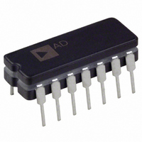
AD637JQ Analog Devices Inc, AD637JQ Datasheet

AD637JQ
Specifications of AD637JQ
Available stocks
Related parts for AD637JQ
AD637JQ Summary of contents
Page 1
FEATURES High accuracy 0.02% maximum nonlinearity rms input 0.10% additional error to crest factor of 3 Wide bandwidth 8 MHz rms input 600 kHz at 100 mV rms Computes True rms Square ...
Page 2
AD637 TABLE OF CONTENTS Features .............................................................................................. 1 Functional Block Diagram .............................................................. 1 General Description ......................................................................... 1 Revision History ............................................................................... 2 Specifications..................................................................................... 3 Absolute Maximum Ratings............................................................ 5 ESD Caution.................................................................................. 5 Pin Configurations and Function Descriptions ........................... 6 Functional Description .................................................................... 7 ...
Page 3
SPECIFICATIONS At 25°C and ±15 V dc, unless otherwise noted. Table 1. AD637J/AD637A Parameter Min Typ TRANSFER FUNCTION V = OUT CONVERSION ACCURACY 2 Total Error, Internal Trim Figure MIN MAX vs. Supply 30 ...
Page 4
AD637 AD637J/AD637A Parameter Min Typ OUTPUT CHARACTERISTICS Offset Voltage vs. Temperature ±0.05 Voltage Swing, 13 12.0 ±15 V Supply, 2 kΩ Load Voltage Swing, 2 ±3 V Supply, 2 kΩ Load Output Current 6 Short-Circuit ...
Page 5
ABSOLUTE MAXIMUM RATINGS Table 2. Parameter ESD Rating Supply Voltage Internal Quiescent Power Dissipation Output Short-Circuit Duration Storage Temperature Range Lead Temperature (Soldering 10 sec) Rated Operating Temperature Range AD637J, AD637K AD637A, AD637B AD637S, 5962-8963701CA Stresses above those listed under ...
Page 6
AD637 PIN CONFIGURATIONS AND FUNCTION DESCRIPTIONS BUFF AD637 COMMON 3 OUTPUT OFFSET TOP VIEW 4 (Not to Scale DEN INPUT 6 dB OUTPUT CONNECT Figure 2. 14-Lead SBDIP/CERDIP Pin Configuration ...
Page 7
FUNCTIONAL DESCRIPTION BUFF OUT 14 1 BUFF IN 24kΩ ABSOLUTE VALUE VOLTAGE TO CURRENT CONVERTER 6kΩ 12kΩ The AD637 embodies an implicit solution of the rms equation that overcomes the inherent limitations of straightforward rms computation. ...
Page 8
AD637 STANDARD CONNECTION The AD637 is simple to connect for a majority of rms measurements. In the standard rms connection shown in Figure 5, only a single external capacitor is required to set the averaging time constant. In this configuration, ...
Page 9
AD637K MAX 2.5 0 EXTERNAL TRIM –2.5 AD637K: 0.5mV ± 0.2% 0.25mV ± 0.05% EXTERNAL –5.0 0 0.5 1.0 INPUT LEVEL (V) Figure 7. Maximum Total Error vs. Input Level AD637K Internal and External Trims AD637 1 BUFF IN ...
Page 10
AD637 AD637 1 BUFF ABSOLUTE VALUE 3 COMMON SQUARER/ OUTPUT DIVIDER 4 OFFSET BIAS +V 4.7kΩ 25kΩ DEN 25kΩ 6 INPUT 7 dB OUTPUT RX 24kΩ Figure 11. 2-Pole Sallen-Key Filter Figure ...
Page 11
Table 5. Practical Values of C and C2 for Various Input Waveforms AV Absolute Value Input Waveform Circuit Waveform and Period and Period T 1/ Symmetrical Sine Wave Sine Wave with dc Offset T ...
Page 12
AD637 AC MEASUREMENT ACCURACY AND CREST FACTOR Crest factor is often overlooked in determining the accuracy measurement. Crest factor is defined as the ratio of the peak signal amplitude to the rms value of the signal (CF ...
Page 13
CALIBRATION Refer to Figure 20: • Set 1.00 V rms IN • Adjust R1 for 0 dB out = 0.00 V • Set 0.10 V rms IN ...
Page 14
AD637 OUTPUT 1MΩ 4 OFFSET 50kΩ ADJUST + –V S 4.7kΩ NOTES 1. VALUES CHOSEN TO GIVE 0.1% AVERAGING ERROR @ 1Hz CONNECT. LOW FREQUENCY MEASUREMENTS If ...
Page 15
EXPANDABLE BUFFER AD637 IC1 BUFF IN 1 ABSOLUTE 2 NC VALUE 3 COMMON BIAS OUTPUT SECTION 4 OFFSET SQUARER/DIVIDER + 4.7kΩ 25kΩ 6 DEN INPUT FILTER 7 dB OUTPUT BUFFER AD637 IC2 BUFF ...
Page 16
AD637 EVALUATION BOARD Figure 23 shows a digital image of the AD637-EVALZ, an evaluation board specially designed for the AD637 available at www.analog.com and is fully tested and ready for bench testing after connecting power and signal I/O. ...
Page 17
Figure 24. AD637-EVALZ Assembly Figure 25. Component Side Silkscreen Figure 26. Evaluation Board—Component Side Copper Figure 27. Evaluation Board—Secondary Side Copper Figure 28. Evaluation Board—Internal Power Plane Figure 29. Evaluation Board—Internal Ground Plane Rev Page ...
Page 18
AD637 GND1 GND2 GND3 GND4 + 50kΩ +V – CF2 47µF 25V POWER SUPPLY – 10µF 10µF 25V 25V + – FILTER BUF_IN 4 OUT 1 2 ...
Page 19
OUTLINE DIMENSIONS 0.005 (0.13) MIN 0.080 (2.03) MAX 14 8 0.310 (7.87) 0.220 (5.59 PIN 1 0.100 (2.54) BSC 0.765 (19.43) MAX 0.060 (1.52) 0.200 (5.08) MAX 0.015 (0.38) 0.150 (3.81) 0.200 (5.08) MIN 0.125 (3.18) SEATING 0.070 ...
Page 20
... PARENTHESES) ARE ROUNDED-OFF MILLIMETER EQUIVALENTS FOR REFERENCE ONLY AND ARE NOT APPROPRIATE FOR USE IN DESIGN. ORDERING GUIDE 1 Model Notes 5962-8963701CA 2 AD637AQ AD637AR AD637ARZ AD637BQ AD637BR AD637BRZ AD637JD AD637JDZ AD637JQ AD637JR AD637JR-REEL AD637JR-REEL7 AD637JRZ AD637JRZ-RL AD637JRZ-R7 AD637KD AD637KDZ AD637KQ AD637KRZ AD637SD AD637SD/883B AD637SQ/883B AD637-EVALZ RoHS Compliant Part ...


