AD637JQ Analog Devices Inc, AD637JQ Datasheet - Page 6
AD637JQ
Manufacturer Part Number
AD637JQ
Description
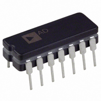
IC RMS/DC CONV PRECISION 14-CDIP
Manufacturer
Analog Devices Inc
Specifications of AD637JQ
Rohs Status
RoHS non-compliant
Current - Supply
2.2mA
Voltage - Supply
±3.0V ~ 18V
Mounting Type
Through Hole
Package / Case
14-CDIP (0.300", 7.62mm)
Accuracy %
0.25%
Bandwidth
200kHz
Supply Current
2.2mA
Power Dissipation Pd
108mW
Supply Voltage Range
± 3V To ± 18V
Digital Ic Case Style
DIP
No. Of Pins
14
Input Type
RMS
Module Type
Converter
Output Type
DC
Voltage, Supply
± 18 VDC
For Use With
AD637-EVALZ - BOARD EVALUATION FOR AD637
Lead Free Status / RoHS Status
Contains lead / RoHS non-compliant
Available stocks
Company
Part Number
Manufacturer
Quantity
Price

Part Number:
AD637JQ
Manufacturer:
ADI/亚德诺
Quantity:
20 000
Company:
Part Number:
AD637JQZ
Manufacturer:
NS
Quantity:
6 221


PIN CONFIGURATIONS AND FUNCTION DESCRIPTIONS
Table 3. 14-Lead SBDIP/CERDIP Pin Function Descriptions
Pin No.
1
2, 12
3
4
5
6
7
8
9
10
11
13
14
AD637
Mnemonic
BUFF IN
NC
COMMON
OUTPUT OFFSET
CS
DEN INPUT
dB OUTPUT
C
RMS OUT
−V
+V
V
BUFF OUT
Figure 2. 14-Lead SBDIP/CERDIP Pin Configuration
IN
AV
OUTPUT OFFSET
S
S
dB OUTPUT
DEN INPUT
COMMON
BUFF IN
NC
CS
1
2
3
4
5
6
7
NC = NO CONNECT
(Not to Scale)
Description
Buffer Input
No Connection
Analog Common
Output Offset
Chip Select
Denominator Input
dB Output
Averaging Capacitor Connection
RMS Output
Negative Supply Rail
Positive Supply Rail
Signal Input
Buffer Output
TOP VIEW
AD637
14
13
12
11
10
9
8
BUFF OUT
V
NC
+V
–V
RMS OUT
C
IN
AV
S
S
Rev. K | Page 6 of 20
Table 4. 16-Lead SOIC_W Pin Function Descriptions
Pin No.
1
2, 8, 9, 14
3
4
5
6
7
10
11
12
13
15
16
Mnemonic
BUFF IN
NC
COMMON
OUTPUT OFFSET
CS
DEN INPUT
dB OUTPUT
C
RMS OUT
−V
+V
V
BUFF OUT
OUTPUT OFFSET
AV
IN
Figure 3. 16-Lead SOIC_W Pin Configuration
S
S
dB OUTPUT
DEN INPUT
COMMON
BUFF IN
NC
NC
CS
1
2
3
4
5
6
7
8
NC = NO CONNECT
(Not to Scale)
TOP VIEW
AD637
Description
Buffer Input
No Connection
Analog Common
Output Offset
Chip Select
Denominator Input
dB Output
Averaging Capacitor Connection
RMS Output
Negative Supply Rail
Positive Supply Rail
Signal Input
Buffer Output
16
15
14
13
12
11
10
9
BUFF OUT
V
NC
+V
–V
RMS OUT
C
NC
IN
AV
S
S
Related parts for AD637JQ
Image
Part Number
Description
Manufacturer
Datasheet
Request
R

Part Number:
Description:
BOARD EVALUATION FOR AD637
Manufacturer:
Analog Devices Inc
Datasheet:

Part Number:
Description:
±1.7g Dual-Axis IMEMS Accelerometer Evaluation Board
Manufacturer:
Analog Devices Inc
Datasheet:
Part Number:
Description:
Inertial Sensor Evaluation System
Manufacturer:
Analog Devices Inc
Datasheet:
Part Number:
Description:
Manufacturer:
Analog Devices Inc
Datasheet:
Part Number:
Description:
Manufacturer:
Analog Devices Inc
Datasheet:
Part Number:
Description:
Manufacturer:
Analog Devices Inc
Datasheet:
Part Number:
Description:
Manufacturer:
Analog Devices Inc
Datasheet:
Part Number:
Description:
Manufacturer:
Analog Devices Inc
Datasheet:
Part Number:
Description:
Manufacturer:
Analog Devices Inc
Datasheet:
Part Number:
Description:
Manufacturer:
Analog Devices Inc
Datasheet:
Part Number:
Description:
Manufacturer:
Analog Devices Inc
Datasheet:
Part Number:
Description:
Manufacturer:
Analog Devices Inc
Datasheet:
Part Number:
Description:
Manufacturer:
Analog Devices Inc
Datasheet: