AD536AKD Analog Devices Inc, AD536AKD Datasheet - Page 9
AD536AKD
Manufacturer Part Number
AD536AKD
Description
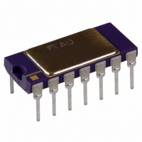
IC TRUE RMS/DC CONV 14-CDIP
Manufacturer
Analog Devices Inc
Datasheet
1.AD536AJHZ.pdf
(16 pages)
Specifications of AD536AKD
Rohs Status
RoHS non-compliant
Current - Supply
1.2mA
Voltage - Supply
5.0V ~ 36V, ±3.0V ~ 18V
Mounting Type
Through Hole
Package / Case
14-CDIP (0.300", 7.62mm)
Accuracy %
0.2%
Bandwidth
450kHz
Supply Current
1.2mA
Power Dissipation Pd
500mW
Supply Voltage Range
5V To 36V
Digital Ic Case Style
DIP
No. Of Pins
14
Lead Free Status / RoHS Status
Contains lead / RoHS non-compliant
Available stocks
Company
Part Number
Manufacturer
Quantity
Price

Part Number:
AD536AKD
Manufacturer:
ADI/亚德诺
Quantity:
20 000
Company:
Part Number:
AD536AKDZ
Manufacturer:
Analog Devices Inc
Quantity:
135


SINGLE-SUPPLY OPERATION
Dual power supplies are shown in Figure 6, Figure 7, Figure 8,
and Figure 9. The AD536A can also be powered by a single
supply greater than 5 V, as shown in Figure 10. When using the
AD536A with a single supply, the differential input stage must
be biased above ground, and the input must be ac coupled.
Biasing the device between the supply and ground is simply a
matter of connecting Pin 10 (COM, Pin 2 on the H-10 package)
to a resistor divider and bypassing the pin to ground. To minimize
power consumption, the values of the resistors may be large, as
Pin 10 current is only 5 μA.
AC input coupling requires only Capacitor C2. A dc return is
not necessary because it is provided internally. C2 is selected for
the proper low frequency breakpoint with the input resistance
of 16.7 kΩ; for a cutoff at 10 Hz, C2 should be 1 μF. The signal
ranges in this connection are slightly more restricted than in the
dual-supply connection. The input and output signal ranges are
shown in Figure 21 and Figure 22. The load resistor, R
essary to provide output sink current.
V
NONPOLARIZED
IN
V
OUT
R
V
V
IN
L
FACTOR
OUT
ADJUST
SCALE
–V
500Ω
Figure 9. Optional External Gain and Output Offset Trims
10kΩ
BUF OUT
1kΩ
R1
TO
S
BUF IN
BUF OUT
1µF
C2
C
BUF IN
–V
dB
V
AV
NC
IN
C
S
–V
V
dB
NC
AV
Figure 10. Single-Supply Connection
IN
1
2
3
4
5
6
7
S
1
2
3
4
5
6
7
AD536A
AD536A
BUF
25kΩ
ABSOLUTE
SQUARER/
BUF
CURRENT
DIVIDER
MIRROR
VALUE
25kΩ
ABSOLUTE
C
SQUARER/
CURRENT
AV
DIVIDER
MIRROR
VALUE
C
AV
25kΩ
25kΩ
14
13
12
11
10
9
8
14
13
12
11
10
9
8
+V
NC
NC
NC
COM
R
I
OUT
L
S
+V
NC
NC
NC
COM
R
I
OUT
L
S
+V
R3
750kΩ
+V
–V
365Ω
S
+V
0.1µF
R2
S
S
S
R4
50kΩ
L
, is nec-
20kΩ
10kΩ
OFFSET
ADJUST
0.1µF
Rev. D | Page 9 of 16
CHOOSING THE AVERAGING TIME CONSTANT
The AD536A computes the rms of both ac and dc signals. If the
input is a slowly varying dc signal, the output of the AD536A
tracks the input exactly.
At higher frequencies, the average output of the AD536A
approaches the rms value of the input signal. The actual output
of the AD536A differs from the ideal output by a dc (or average)
error and some amount of ripple, as shown in Figure 11.
The dc error is dependent on the input signal frequency and
the value of C
of C
frequency using the standard rms connection.
The ac component of the output signal is the ripple. There are
two ways to reduce the ripple. The first method involves using a
large value of C
to C
reduction in ripple.
When measuring waveforms with high crest factors, such as low
duty cycle pulse trains, the averaging time constant should be at
least 10 times the signal period. For example, a 100 Hz pulse
rate requires a 100 ms time constant, which corresponds to a
4 μF capacitor (time constant = 25 ms per μF).
AV
AV
, which yields a given percentage of dc error above a given
, a tenfold increase in this capacitance affects a tenfold
E
O
Figure 11. Typical Output Waveform for Sinusoidal Input
AV
. Use Figure 12 to determine the minimum value
AV
. Because the ripple is inversely proportional
DOUBLE FREQUENCY
RIPPLE
IDEAL E
DC ERROR = E
O
O
AVERAGE E
– E
O
(IDEAL)
TIME
O
AD536A
– E
O
Related parts for AD536AKD
Image
Part Number
Description
Manufacturer
Datasheet
Request
R

Part Number:
Description:
±1.7g Dual-Axis IMEMS Accelerometer Evaluation Board
Manufacturer:
Analog Devices Inc
Datasheet:

Part Number:
Description:
Inertial Sensor Evaluation System
Manufacturer:
Analog Devices Inc
Datasheet:
Part Number:
Description:
Manufacturer:
Analog Devices Inc
Datasheet:
Part Number:
Description:
Manufacturer:
Analog Devices Inc
Datasheet:
Part Number:
Description:
Manufacturer:
Analog Devices Inc
Datasheet:
Part Number:
Description:
Manufacturer:
Analog Devices Inc
Datasheet:
Part Number:
Description:
Manufacturer:
Analog Devices Inc
Datasheet:
Part Number:
Description:
Manufacturer:
Analog Devices Inc
Datasheet:
Part Number:
Description:
Manufacturer:
Analog Devices Inc
Datasheet:
Part Number:
Description:
Manufacturer:
Analog Devices Inc
Datasheet:
Part Number:
Description:
Manufacturer:
Analog Devices Inc
Datasheet:
Part Number:
Description:
Manufacturer:
Analog Devices Inc
Datasheet:
Part Number:
Description:
Manufacturer:
Analog Devices Inc
Datasheet: