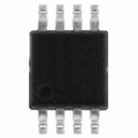
STTS75DS2F STMicroelectronics, STTS75DS2F Datasheet - Page 23

STTS75DS2F
Manufacturer Part Number
STTS75DS2F
Description
IC TEMP SENSOR DGTL WCHDG 8MSOP
Manufacturer
STMicroelectronics
Datasheet
1.STTS75M2F.pdf
(41 pages)
Specifications of STTS75DS2F
Function
Temp Sensor, Watchdog
Topology
ADC (Sigma Delta), Comparator, Register Bank
Sensor Type
Internal
Sensing Temperature
-55°C ~ 125°C
Output Type
I²C™/SMBus™
Output Alarm
Yes
Output Fan
No
Voltage - Supply
2.7 V ~ 5.5 V
Operating Temperature
-55°C ~ 125°C
Mounting Type
Surface Mount
Package / Case
8-MSOP, Micro8™, 8-uMAX, 8-uSOP,
Full Temp Accuracy
+/- 3 C
Digital Output - Bus Interface
Serial (2-Wire, I2C)
Digital Output - Number Of Bits
12 bit
Maximum Operating Temperature
+ 125 C
Minimum Operating Temperature
- 55 C
For Use With
497-8844 - EVAL DAUGHTER STTS75 8-TSSOP497-8419 - BOARD ST72651AR6/STTS75/STLM20
Lead Free Status / RoHS Status
Lead free / RoHS Compliant
Other names
497-6331-2
Available stocks
Company
Part Number
Manufacturer
Quantity
Price
Company:
Part Number:
STTS75DS2F
Manufacturer:
NXP
Quantity:
1 104
Company:
Part Number:
STTS75DS2F
Manufacturer:
STMicroelectronics
Quantity:
1 908
STTS75
3.4.5
Acknowledge
Each byte of eight bits is followed by one acknowledge bit. This acknowledge bit is a low
level put on the bus by the receiver whereas the master generates an extra acknowledge
related clock pulse (see
obliged to generate an acknowledge after the reception of each byte that has been clocked
out of the slave transmitter.
The device that acknowledges has to pull down the SDA line during the acknowledge clock
pulse in such a way that the SDA line is a stable low during the high period of the
acknowledge related clock pulse. Of course, setup and hold times must be taken into
account. A master receiver must signal an end of data to the slave transmitter by not
generating an acknowledge on the last byte that has been clocked out of the slave. In this
case the transmitter must leave the data line high to enable the master to generate the
STOP condition.
Figure 7.
SCL FROM
MASTER
DATA OUTPUT
BY TRANSMITTER
DATA OUTPUT
BY RECEIVER
Acknowledgement sequence
START
Figure 7 on page
MSB
Doc ID 13298 Rev 11
1
23). A slave receiver which is addressed is
2
LSB
8
Functional description
ACKNOWLEDGEMENT
CLOCK PULSE FOR
9
AI00601
23/41


