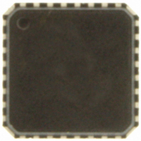
ADT7462ACPZ-5RL7 ON Semiconductor, ADT7462ACPZ-5RL7 Datasheet - Page 17

ADT7462ACPZ-5RL7
Manufacturer Part Number
ADT7462ACPZ-5RL7
Description
IC TEMP/VOLT MONITOR 32-LFCSP
Manufacturer
ON Semiconductor
Datasheet
1.ADT7462ACPZ-5RL7.pdf
(81 pages)
Specifications of ADT7462ACPZ-5RL7
Function
Fan Control, Temp Monitor
Topology
ADC, Comparator, Multiplexer, Register Bank
Sensor Type
External & Internal
Sensing Temperature
-40°C ~ 125°C, External Sensor
Output Type
SMBus™
Output Alarm
No
Output Fan
Yes
Voltage - Supply
3 V ~ 5.5 V
Operating Temperature
-40°C ~ 125°C
Mounting Type
Surface Mount
Package / Case
32-LFCSP
Supply Voltage (max)
5.5 V
Supply Voltage (min)
3 V
Maximum Operating Temperature
+ 125 C
Minimum Operating Temperature
- 40 C
Lead Free Status / RoHS Status
Lead free / RoHS Compliant
Other names
ADT7462ACPZ-500RL7
ADT7462ACPZ-500RL7
ADT7462ACPZ-500RL7TR
ADT7462ACPZ-500RL7TR
ADT7462ACPZ-5RL7TR
ADT7462ACPZ-500RL7
ADT7462ACPZ-500RL7TR
ADT7462ACPZ-500RL7TR
ADT7462ACPZ-5RL7TR
Available stocks
Company
Part Number
Manufacturer
Quantity
Price
Company:
Part Number:
ADT7462ACPZ-5RL7
Manufacturer:
ON Semiconductor
Quantity:
135
a register address to RAM for a subsequent single byte read
from the same address. This operation is shown in Figure 27.
after setting up the address, the master can assert a repeat
start condition immediately after the final ACK and carry
out a single byte read without asserting an intermediate stop
condition.
Write Byte
and one data byte to the slave device as follows:
Read Operations
Receive Byte
single register. The register address must be set up
previously. In this operation, the master device receives a
single byte from a slave device as follows:
For the ADT7462, the send byte protocol is used to write
If it is required to read data from the register immediately
In this operation, the master device sends a command byte
The ADT7462 uses the following SMBus read protocols.
The receive byte is useful when repeatedly reading a
1. The master device asserts a start condition on SDA.
2. The master sends the 7−bit slave address followed
3. The addressed slave device asserts an ACK on SDA.
4. The master sends a command code.
5. The slave asserts an ACK on SDA.
6. The master sends a data byte.
7. The slave asserts an ACK on SDA.
8. The master asserts a stop condition on SDA to end
1. The master device asserts a start condition on SDA.
2. The master sends the 7−bit slave address followed
3. The addressed slave device asserts an ACK on SDA.
4. The master receives a data byte.
5. The master asserts a NO ACK on SDA.
6. The master asserts a stop condition on SDA to end
Figure 28. Single−Byte Write to a Register
Figure 27. Setting a Register Address for
by the write bit (low).
the transaction.
by the read bit (high).
the transaction.
S
1
ADDRESS W A
SLAVE
S
1
2
ADDRESS
SLAVE
Subsequent Read
2
3
W A
ADDRESS
3
SLAVE
1
S
4
ADDRESS
REGISTER
ADDRESS
SLAVE
2
4
A
5
W A
DATA
A P
5 6
6
3
Figure 29. Block Write to ADT7462
COMMAND
7 8
A P
BLOCK
WRITE
0xA0
4
http://onsemi.com
A
5
COUNT
BYTE
6
17
A DATA 1 A
7
Block Write
to a slave device. The start address for a block write must be
set previously. In the case of the ADT7462, this is done by
a send byte operation to set a RAM address. The user writes
the number of registers to be written to in the block read
command to the #Bytes bits of the Configuration 0 register.
a single byte of data from a register whose address has
previously been set by a send byte or write a byte operation.
Block Read
from a slave device. The start address for a block read must
be set previously, as well as the number of bytes to be read
(maximum = 32). In the case of the ADT7462, the start
address is activated by a send byte operation to set a RAM
address. The number of bytes to be read should be written to
8
In this operation, the master device writes a block of data
For the ADT7462, the receive byte protocol is used to read
In this operation, the master device reads a block of data
10. The master asserts a stop condition on SDA to end
9
1. The master device asserts a start condition on SDA.
2. The master sends the 7−bit slave address followed
3. The addressed slave device asserts an ACK on SDA.
4. The master sends a command code that tells the
5. The slave asserts an ACK on SDA.
6. The master sends the data bytes (the number of
7. The slave asserts an ACK on SDA after each data
8. The master sends a packet error checking (PEC) byte.
9. The ADT7462 checks the PEC byte and issues an
Figure 30. Single−Byte Read from a Register
DATA 2 A DATA
by the write bit (low).
slave device to expect a block write. The
ADT7462 command code for a block write is
0xA0 (1010 0000).
data bytes sent is written to the #Bytes bits of the
Configuration 0 register).
byte.
ACK, if correct. If incorrect (NO ACK), the
master resends the data bytes.
the transaction.
32
1
S
ADDRESS
SLAVE
A
PEC
2
10
11 12
A P
R
3
A
DATA
4
A P
5 6


