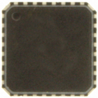
ADT7462ACPZ-5RL7 ON Semiconductor, ADT7462ACPZ-5RL7 Datasheet - Page 50

ADT7462ACPZ-5RL7
Manufacturer Part Number
ADT7462ACPZ-5RL7
Description
IC TEMP/VOLT MONITOR 32-LFCSP
Manufacturer
ON Semiconductor
Datasheet
1.ADT7462ACPZ-5RL7.pdf
(81 pages)
Specifications of ADT7462ACPZ-5RL7
Function
Fan Control, Temp Monitor
Topology
ADC, Comparator, Multiplexer, Register Bank
Sensor Type
External & Internal
Sensing Temperature
-40°C ~ 125°C, External Sensor
Output Type
SMBus™
Output Alarm
No
Output Fan
Yes
Voltage - Supply
3 V ~ 5.5 V
Operating Temperature
-40°C ~ 125°C
Mounting Type
Surface Mount
Package / Case
32-LFCSP
Supply Voltage (max)
5.5 V
Supply Voltage (min)
3 V
Maximum Operating Temperature
+ 125 C
Minimum Operating Temperature
- 40 C
Lead Free Status / RoHS Status
Lead free / RoHS Compliant
Other names
ADT7462ACPZ-500RL7
ADT7462ACPZ-500RL7
ADT7462ACPZ-500RL7TR
ADT7462ACPZ-500RL7TR
ADT7462ACPZ-5RL7TR
ADT7462ACPZ-500RL7
ADT7462ACPZ-500RL7TR
ADT7462ACPZ-500RL7TR
ADT7462ACPZ-5RL7TR
Available stocks
Company
Part Number
Manufacturer
Quantity
Price
Company:
Part Number:
ADT7462ACPZ-5RL7
Manufacturer:
ON Semiconductor
Quantity:
135
(0xB9) are set to Logic 1 whenever the THERM input is
asserted low. The THERM state bits in Host Thermal Status
Register 2 (0xB9) indicate that a high−to−low transition has
taken place on the THERM pin.
THERM Timer
THERM inputs as a percentage of a timer window. The timer
window for the THERM1 input is programmed using Bits
[4:2] of the THERM configuration register (0x0D). The
timer window for the THERM2 input is programmed using
Bits [7:5] of the THERM configuration register (0x0D).
Values from 0.25 sec to 8 sec are programmable (see
Table 27).
stored in the THERM % on−time registers. This is a
cumulative sum of the percentage of time during the
THERM timer window that THERM is asserted. The %
on−time and associated timer limit registers are listed in
Table 28.
TEMPERATURE
1005C
ALERT
THERM
905C
805C
705C
605C
505C
405C
Table 27. THERM Timer Window
Table 28. THERM On−Time and Timer Limit Register
THERM1
THERM2
Channel
The ADT7462 can also measure assertion times on the
The assertion time as a percentage of the timer window is
Code
000
001
010
100
101
011
110
111
1
% On−Time Register
Figure 83. THERM Behavior
2
0xAE
0xAF
THERM Timer Window
3
% Timer Limit Register
RESET BY MASTER
0.25 sec
0.5 sec
1 sec
2 sec
4 sec
8 sec
8 sec
8 sec
4
0x80
0x81
THERM LIMIT
HIGH TEMP LIMIT
THERM LIMIT
HYSTERESIS
http://onsemi.com
50
corresponding percentage limit, the T1% bit in Host
Thermal Status Register 2 (0xB9) is asserted, and an ALERT
is generated (that is, if the mask bit is not set). If the limit is
set to 0x00, an ALERT is generated on the first assertion. If
the limit is set to 0xFF, an ALERT is never generated
because 0xFF corresponds to the THERM input being
asserted all the time.
[4:1] of the THERM zone in the THERM1 configuration
register (0x0E) and the THERM2 configuration register
(0x0F) allows Pin 28/Pin 29 to operate as an I/O.
THERM Timer Limit Register
and Register 0x81. If THERM is asserted for longer than the
programmed percentage limit, then an ALERT is generated.
The limit is programmed as a percentage of the chosen
THERM timer window.
EXAMPLE: The THERM timer window is eight seconds,
and an ALERT should be generated if THERM is asserted
for more than one second.
The THERM timer limit register is an 8−bit register.
Therefore, 1 LSB = 0.39%
has been exceeded, then an ALERT is generated.
General−Purpose I/O Pins
GPIO4 can be configured to enable event driven outputs
(EDOs), and GPIO5 and GPIO6 can act as EDOs, if the EDO
functionality is enabled. Two other GPIOs (GPIO7 and
GPIO8) are standard GPIO pins that are dedicated to
general−purpose logic input/output.
bits in a GPIO configuration register (0x09 and 0x0A), one
in the GPIO status register (0xBF), and one in the GPIO
mask register (0x36).
makes the corresponding GPIO pin an output.
GPIO pin an input.
makes the corresponding GPIO pin active high.
GPIO pin active low.
corresponding bit in the GPIO status register is read−only,
and it is set when the input is asserted (“asserted” can be high
or low, depending on the setting of the polarity bit).
When
When THERM is configured as an input only, setting Bits
The THERM timer limit is programmed to Register 0x80
When the time window has elapsed, if the THERM limit
The ADT7462 has eight open−drain GPIO pins. GPIO1 to
Each GPIO pin has five data bits associated with it: three
Setting a direction bit to 1 in a GPIO configuration register
Clearing the direction bit to 0 makes the corresponding
Setting a polarity bit to 1 in a GPIO configuration register
Clearing the polarity bit to 0 makes the corresponding
When a GPIO pin is configured as an input, the
the
12.5%
0.39%
measured
+ 32 decimal + 0
0
%Limit + 1
00 + 0%; 0
percentage
8
20 + 00100000
100 + 12.5%
exceeds
FF + 100%
the


