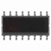
L6910 STMicroelectronics, L6910 Datasheet - Page 11

L6910
Manufacturer Part Number
L6910
Description
IC PWM BUCK BST VM 16SOIC
Manufacturer
STMicroelectronics
Datasheet
1.L6910ATR.pdf
(29 pages)
Specifications of L6910
Pwm Type
Voltage Mode
Number Of Outputs
1
Frequency - Max
230kHz
Duty Cycle
100%
Voltage - Supply
5 V ~ 12 V
Buck
Yes
Boost
Yes
Flyback
No
Inverting
No
Doubler
No
Divider
No
Cuk
No
Isolated
No
Operating Temperature
-40°C ~ 150°C
Package / Case
16-SOIC (3.9mm Width)
Frequency-max
230kHz
Output Voltage
4 V
Mounting Style
SMD/SMT
Lead Free Status / RoHS Status
Contains lead / RoHS non-compliant
Other names
497-3656-5
497-4220-5
497-4220-5
497-4220-5
497-4220-5
Available stocks
Company
Part Number
Manufacturer
Quantity
Price
Part Number:
L6910
Manufacturer:
ST
Quantity:
20 000
Part Number:
L6910A
Manufacturer:
ST
Quantity:
20 000
Company:
Part Number:
L6910ATR
Manufacturer:
INF
Quantity:
2 523
Part Number:
L6910ATR
Manufacturer:
ST
Quantity:
20 000
Figure 11. Asymptotic Bode Plot of Converter's Gain
5
The demo board shows the operation of the device in a general purpose application. This evaluation board al-
lows voltage adjustability from 0.9V to 5V through the switches S2-S5 according to the reported table when the
internal 0.9V reference is used (G1 closed). Output current in excess of 20A can be reached dependently on
the kind of mosfet used: up to three SO8 mosfet may be used for both High side and Low side switches. External
reference may be used for the regulation simply leaving open G1 and the switches S2-S5. The device may also
be disabled with the switch S1. The V
the V
to be closed and a 5V to 12V input can be directly connected to the V
copper thickness is of 70 m in order to minimize conduction losses considering the high current that the circuit
is able to deliver.The PGOOD signal is used as a logic level and it's been pulled up to V
other appropriate voltage available on the demo board. In case of input voltage higher than 7V (PGOOD Pin
Maximum Absolute Rating) a 5V reference is required. Figure 12 shows the demo board's schematic circuit
Figure 12. 15A Demo Board Schematic
15A DEMO BOARD DESCRIPTION
IN
input rail. The device is also able to operate with a single supply voltage; in this case the jumper G2 has
GNDREFIN
GNDREF
GNDCC
GNDIN
+VREF
REFIN
VCC
VIN
S1
S2
S3
S4
S5
F1
C17
G2
C16
C12
R6
SR12
SR13
C21
R10
R11
G1
R1
EAREF
VREF
GND
OSC
V
C15
SS
CC
D1
dB
COMP
CC
15
7
8
1
4
2
Modulator Gain
Compensation Network Gain
Error Amplifier
BOOT
R5/R3
L1
input rail supplies the device while the power conversion starts from
5
C19
12
D03IN1513
Error Amplifier
OCSET
R5
C18
R7
VFB
3
6
11
10
14
13
9
LC
C13
C14
UGATE
PHASE
LGATE
PGND
PGOOD
R4
Closed Loop Gain
R3
C20
ESR
Q1-3
Q4-6
P1
P2
IN
D2
R8
V
0.9
1.2
1.5
1.8
2.5
3.3
5.0
OUT
input. The four layers demo board's
C1-C3
Open Open Open Open
Open
Open Open ON Open
Open Open Open ON
Open Open ON
C22
ON Open Open Open
ON
R9
L2
S2
ON
ON Open Open
S3
C4-
11
Open Open
S4
ON
S5
IN
R2
L6910 - L6910A
because there's no
V
GNDOUT
PWRGD
OUT
11/29


