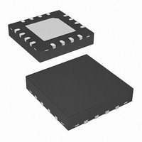
ISL6269BCRZ Intersil, ISL6269BCRZ Datasheet - Page 11

ISL6269BCRZ
Manufacturer Part Number
ISL6269BCRZ
Description
IC PWM CTRLR SYNC BUCK 16-QFN
Manufacturer
Intersil
Datasheet
1.ISL6269BCRZ.pdf
(14 pages)
Specifications of ISL6269BCRZ
Pwm Type
Controller
Number Of Outputs
1
Frequency - Max
600kHz
Voltage - Supply
5 V ~ 25 V
Buck
Yes
Boost
No
Flyback
No
Inverting
No
Doubler
No
Divider
No
Cuk
No
Isolated
No
Operating Temperature
-10°C ~ 100°C
Package / Case
16-VQFN Exposed Pad, 16-HVQFN, 16-SQFN, 16-DHVQFN
Frequency-max
600kHz
Lead Free Status / RoHS Status
Lead free / RoHS Compliant
Duty Cycle
-
General Application Design Guide
This design guide is intended to provide a high-level
explanation of the steps necessary to create a single-phase
power converter. It is assumed that the reader is familiar with
many of the basic skills and techniques referenced below. In
addition to this guide, Intersil provides complete reference
designs that include schematics, bills of materials, and
example board layouts.
Selecting the LC Output Filter
The duty cycle of an ideal buck converter is a function of the
input and the output voltage. This relationship is written as:
The output inductor peak-to-peak ripple current is written as:
I
A typical step-down DC/DC converter will have an I
20% to 40% of the maximum DC output load current. The
value of I
MOSFET switching loss, inductor core loss, and the resistive
loss of the inductor winding. The DC copper loss of the
inductor can be estimated by:
Where I
The copper loss can be significant so attention has to be
given to the DCR selection. Another factor to consider when
choosing the inductor is its saturation characteristics at
elevated temperature. A saturated inductor could cause
destruction of circuit components, as well as nuisance OCP
faults.
A DC/DC buck regulator must have output capacitance
C
develops a corresponding ripple voltage V
which is the sum of the voltage drop across the capacitor
ESR and of the voltage change stemming from charge
moved in and out of the capacitor. These two voltages are
written as:
and
If the output of the converter has to support a load with high
pulsating current, several capacitors will need to be paralleled
to reduce the total ESR until the required V
The inductance of the capacitor can cause a brief voltage dip
if the load transient has an extremely high slew rate. Low
inductance capacitors constructed with reverse package
geometry are available. A capacitor dissipates heat as a
function of RMS current and frequency. Be sure that I
D
P
ΔV
ΔV
PP
COPPER
OUT
=
ESR
C
=
V
--------------- -
=
V
OUT
V
------------------------------------- -
into which ripple current I
IN
OUT
f
------------------------------------ -
8 C
LOAD
=
SW
PP
•
I
PP
=
OUT
•
•
L
is selected based upon several criteria such as
I
(
I
PP
LOAD
•
1 D
OUT
is the converter output DC current.
E
–
SR
•
f
SW
)
2
•
DCR
11
PP
can flow. Current I
PP
PP
is achieved.
across C
PP
PP
(EQ. 12)
(EQ. 13)
(EQ. 10)
(EQ. 11)
PP
(EQ. 9)
OUT,
of
is
ISL6269B
shared by a sufficient quantity of paralleled capacitors so that
they operate below the maximum rated RMS current at f
Take into account that the rated value of a capacitor can fade
as much as 50% as the DC voltage across it increases.
Selection of the Input Capacitor
The important parameters for the bulk input capacitance are
the voltage rating and the RMS current rating. For reliable
operation, select bulk capacitors with voltage and current
ratings above the maximum input voltage and capable of
supplying the RMS current required by the switching circuit.
Their voltage rating should be at least 1.25 times greater
than the maximum input voltage, while a voltage rating of 1.5
times is a preferred rating. Figure 7 is a graph of the input
RMS ripple current, normalized relative to output load current,
as a function of duty cycle that is adjusted for converter
efficiency. The ripple current calculation is written as:
Where:
In addition to the bulk capacitance, some low ESL ceramic
capacitance is recommended to decouple between the drain
of the high-side MOSFET and the source of the low-side
MOSFET.
I
IN_RMS
D
FIGURE 7. NORMALIZED RMS INPUT CURRENT FOR x = 0.8
- I
- x is a multiplier (0 to 1) corresponding to the inductor
- D is the duty cycle that is adjusted to take into account
=
peak-to-peak ripple amplitude expressed as a
percentage of I
the efficiency of the converter which is written as:
0.60
0.55
0.50
0.45
0.40
0.35
0.30
0.25
0.20
0.15
0.10
0.05
MAX
------------------------- -
V
0
IN
V
0
=
OUT
⋅
is the maximum continuous I
EFF
---------------------------------------------------------------------------------------------------- -
0.1
(
I
MAX
0.2
2
MAX
⋅
(
D D
0.3
–
(0% to 100%)
I
MAX
2
0.4
x = 1
x = 0.75
x = 0.50
x = 0.25
x = 0
DUTY CYCLE
)
)
+
⎛
⎝
0.5
x I
⋅
MAX
0.6
LOAD
2
⋅
----- -
12
0.7
D
⎞
⎠
of the converter
0.8
May 30, 2007
0.9
(EQ. 14)
(EQ. 15)
FN6280.2
SW
1
.


