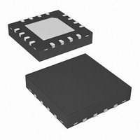
ISL6269BCRZ Intersil, ISL6269BCRZ Datasheet - Page 6

ISL6269BCRZ
Manufacturer Part Number
ISL6269BCRZ
Description
IC PWM CTRLR SYNC BUCK 16-QFN
Manufacturer
Intersil
Datasheet
1.ISL6269BCRZ.pdf
(14 pages)
Specifications of ISL6269BCRZ
Pwm Type
Controller
Number Of Outputs
1
Frequency - Max
600kHz
Voltage - Supply
5 V ~ 25 V
Buck
Yes
Boost
No
Flyback
No
Inverting
No
Doubler
No
Divider
No
Cuk
No
Isolated
No
Operating Temperature
-10°C ~ 100°C
Package / Case
16-VQFN Exposed Pad, 16-HVQFN, 16-SQFN, 16-DHVQFN
Frequency-max
600kHz
Lead Free Status / RoHS Status
Lead free / RoHS Compliant
Duty Cycle
-
Electrical Specifications
NOTE:
Functional Pin Descriptions
GND (Bottom Pad)
Signal common of the IC. Unless otherwise stated, signals
are referenced to the GND pin, not the PGND pin.
VIN (Pin 1)
The VIN pin measures the converter input voltage which is a
required input to the R
the drain of the high-side MOSFET to the GND pin.
VCC (Pin 2)
The VCC pin is the input bias voltage for the IC. Connect
+5V from the VCC pin to the GND pin. Decouple with at least
1µF of a MLCC capacitor from the VCC pin to the GND pin.
FCCM (Pin 3)
The FCCM pin configures the controller to operate in forced-
continuous-conduction-mode (FCCM) or diode-emulation-
mode (DEM.) DEM is disabled when the FCCM pin is pulled
above the rising threshold voltage V
DEM is enabled when the FCCM pin is pulled below the
falling threshold voltage V
EN (Pin 4)
The EN pin is the on/off switch of the IC. The soft-start
sequence begins when the EN pin is pulled above the rising
threshold voltage V
reset (POR) rising threshold voltage
EN pin is pulled below the falling threshold voltage V
PWM immediately stops.
COMP (Pin 5)
The COMP pin is the output of the control-loop error
amplifier. Compensation components for the control-loop
connect across the COMP and FB pins.
FB (Pin 6)
The FB pin is the inverting input of the control-loop error
amplifier. The converter output voltage regulates to 600mV
OTP Hysteresis (Note 3)
PROTECTION
ISEN OCP Threshold
ISEN Short-Circuit Threshold
UVP Threshold
OVP Rising Threshold
OVP Falling Threshold
OTP Rising Threshold (Note 3)
3. Guaranteed by characterization.
PARAMETER
ENTHR
3
PWM modulator. Connect across
FCCMTHF.
and
6
V VCC
These specifications apply for T
All typical specifications T
FCCMTHR
V VCC_THR
is above the power-on
SYMBOL
T
V
V
T
OTHYS
V
I
I
OVR
OTR
OVF
OC
SC
UV
, conversely
. When the
ISEN sourcing, T
ISEN sourcing
ISEN sourcing
ENTHF
A
= +25°C, VCC = 5V, PVCC = 5V, VIN = 15V (Continued)
ISL6269B
A
= -40°C to +100°C, unless otherwise stated.
TEST CONDITIONS
A
= -10°C to +100°C
from the FB pin to the GND pin. Program the desired output
voltage with a resistor network connected across the VO,
FB, and GND pins. Select the resistor values such that FB to
GND is 600mV when the converter output voltage is at the
programmed regulation value.
FSET (Pin 7)
The FSET pin programs the PWM switching frequency.
Program the desired PWM frequency with a resistor and a
capacitor connected across the FSET and GND pins.
VO (Pin 8)
The VO pin measures the converter output voltage and is
used exclusively as an input to the R
Connect at the physical location where the best output
voltage regulation is desired.
ISEN (Pin 9)
The ISEN pin programs the threshold of the OCP
overcurrent fault protection. Program the desired OCP
threshold with a resistor connected across the ISEN and
PHASE pins. The OCP threshold is programmed to detect
the peak current of the output inductor. The peak current is
the sum of the DC and AC components of the inductor
current.
PGND (Pin 10)
The PGND pin conducts the turn-off transient current
through the LG gate driver. The PGND pin must be
connected to complete the pulldown circuit of the LG gate
driver. The PGND pin should be connected to the source of
the low-side MOSFET through a low impedance path,
preferably in parallel with the trace connecting the LG pin to
the gate of the low-side MOSFET. The adaptive shoot-
through protection circuit, measures the low-side MOSFET
gate-source voltage from the LG pin to the PGND pin.
LG (Pin 11)
The LG pin is the output of the low-side MOSFET gate
driver. Connect to the gate of the low-side MOSFET.
MIN
113
100
19
17
81
-
-
-
3
PWM modulator.
TYP
116
103
150
26
26
50
84
25
MAX
119
106
33
33
87
-
-
-
May 30, 2007
FN6280.2
UNIT
μA
μA
μA
°C
°C
%
%
%


