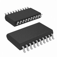
ISL6754AAZA Intersil, ISL6754AAZA Datasheet

ISL6754AAZA
Specifications of ISL6754AAZA
Available stocks
Related parts for ISL6754AAZA
ISL6754AAZA Summary of contents
Page 1
... PART RANGE (Note) MARKING (°C) ISL6754AAZA* 6754 AAZ -40 to +105 20 Ld QSOP M20.15 *Add -T suffix to part number for tape and reel packaging. NOTE: These Intersil Pb-free plastic packaged products employ special Pb-free material sets, molding compounds/die attach materials, and 100% matte tin plate plus anneal (e3 termination finish, which is RoHS compliant and compatible with both SnPb and Pb-free soldering operations) ...
Page 2
Functional Block Diagram VDD VREF UVLO OVER- TEMPERATURE PROTECTION GND VREF RESDEL IOUT 4X OSCILLATOR CT RTD CTBUF SS 50% PWM STEERING LOGIC PWM SAMPLE AND HOLD + - 1.00V OVER CURRENT COMPARATOR VREF PWM COMPARATOR + - 0.33 SOFTSTART ...
Page 3
Typical Application - High Voltage Input Primary Side Control ZVS Full-Bridge Converter VIN+ CR2 R15 Q8A Q8B 400 VDC Q6A Q6B Q4 VIN- T2 CR1 VDD BIAS ...
Page 4
Typical Application - High Voltage Input Secondary Side Control ZVS Full-Bridge Converter VIN CR2 R17 + 400 VDC C1 Q4 CR4 R15 Q7A Q7B C10 VIN- VREF T2 CR1 R12 SECONDARY BIAS SUPPLY C2 C3 ...
Page 5
... Thermal Resistance Junction to Ambient (Typical) 20 Lead QSOP (Note 1 0.3V REF Maximum Junction Temperature . . . . . . . . . . . . . . .-55°C to +150°C Maximum Storage Temperature Range . . . . . . . . . .-65°C to +150°C Pb-Free Reflow Profile .see link below http://www.intersil.com/pbfree/Pb-FreeReflow.asp = +25°C; Parameters with MIN and/or MAX limits are 100% A TEST CONDITIONS ...
Page 6
Electrical Specifications Recommended operating conditions unless otherwise noted. Refer to “Functional Block Diagram” on page 2 and “Typical Application schematics” beginning on page 3. 9V < -40°C to +105°C, Typical values are tested at ...
Page 7
Electrical Specifications Recommended operating conditions unless otherwise noted. Refer to “Functional Block Diagram” on page 2 and “Typical Application schematics” beginning on page 3. 9V < -40°C to +105°C, Typical values are tested at ...
Page 8
Typical Performance Curves 1.02 1.01 1 0.99 0.98 -40 -25 - TEMPERATURE (¬¨Ð FIGURE 1. REFERENCE VOLTAGE vs TEMPERATURE 4 1- 1000pF CT = 1000pF CT = 680pF CT = 680pF CT = 470pF CT ...
Page 9
RC network to produce the desired sawtooth waveform. OUTUL and OUTUR - These outputs control the upper bridge FETs and operate at a fixed 50% duty cycle in alternate sequence. OUTUL controls the upper left FET and OUTUR ...
Page 10
The switching period is the sum of the timing capacitor charge and discharge durations. The charge duration is determined by CT and a fixed 200µA internal current source. The discharge duration is determined by RTD and CT. 3 ≈ ⋅ ...
Page 11
CHANNEL 1 (YELLOW): OUTLL CHANNEL 2 (RED): OUTLR CHANNEL 3 (BLUE): CS CHANNEL 4 (GREEN): IOUT FIGURE 6. DYNAMIC BEHAVIOR The average current signal on I remains accurate OUT provided the output inductor current remains continuous ...
Page 12
If voltage-mode control is used in a bridge topology, it should be noted that peak current limit results in inherently unstable operation. DC blocking capacitors used in voltage-mode bridge topologies become unbalanced, as does the flux in the transformer core. ...
Page 13
Slope Compensation Peak current-mode control requires slope compensation to improve noise immunity, particularly at lighter loads, and to prevent current loop instability, particularly for duty cycles greater than 50%. Slope compensation may be accomplished by summing an external ramp with ...
Page 14
If ΔV is greater than or equal slope compensation is needed and ------------------------------------------------------------------------------------------------------------------------------------- - ⎛ ⎛ ⋅ ⋅ ⋅ ⎜ ⎜ ------- - I ...
Page 15
FIGURE 11. ADDING SLOPE COMPENSATION USING CT Using CT to provide slope compensation instead of CTBUF requires the same calculations, except that Equations 22 and 23 require modification. Equation 22 becomes: ⋅ ΔV ...
Page 16
The power transfer period terminates when switch LR turns off as determined by the PWM. The current flowing in the primary cannot be interrupted instantaneously must find an alternate path. The current flows into the ...
Page 17
UR, the transformer primary, and switch UL. When switch LL opens, the output inductor current free-wheels predominantly through diode D1. Diode D2 may actually conduct very little or none ...
Page 18
CT OUTLL OUTLR OUTLLN (SR1) OUTLRN (SR2) FIGURE 22. WAVEFORM TIMING WITH SR OUTPUTS DELAYED, 2.575V < VADJ < 5.00V Setting VADJ results in no delay on any output. REF The no delay voltage has a ±75mV ...
Page 19
... Accordingly, the reader is cautioned to verify that data sheets are current before placing orders. Information furnished by Intersil is believed to be accurate and reliable. However, no responsibility is assumed by Intersil or its subsidiaries for its use; nor for any infringements of patents or other rights of third parties which may result from its use ...


