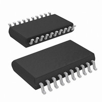
ISL6754AAZA Intersil, ISL6754AAZA Datasheet - Page 10

ISL6754AAZA
Manufacturer Part Number
ISL6754AAZA
Description
IC CTRLR PWM FULL-BRDG 20-QSOP
Manufacturer
Intersil
Datasheet
1.ISL6754AAZA-T.pdf
(19 pages)
Specifications of ISL6754AAZA
Pwm Type
Voltage/Current Mode
Number Of Outputs
6
Frequency - Max
2MHz
Duty Cycle
100%
Voltage - Supply
9 V ~ 16 V
Buck
No
Boost
No
Flyback
No
Inverting
No
Doubler
No
Divider
No
Cuk
No
Isolated
No
Operating Temperature
-40°C ~ 105°C
Package / Case
20-QSOP
Frequency-max
2MHz
Lead Free Status / RoHS Status
Lead free / RoHS Compliant
Available stocks
Company
Part Number
Manufacturer
Quantity
Price
Company:
Part Number:
ISL6754AAZA
Manufacturer:
Intersil
Quantity:
522
Company:
Part Number:
ISL6754AAZA-T
Manufacturer:
Intersil
Quantity:
1 900
The switching period is the sum of the timing capacitor
charge and discharge durations. The charge duration is
determined by CT and a fixed 200µA internal current source.
The discharge duration is determined by RTD and CT.
T
T
T
where T
respectively, CT is the timing capacitor in Farads, RTD is the
discharge programming resistance in ohms, T
oscillator period, and F
output switching cycle requires two oscillator cycles. The
actual times will be slightly longer than calculated due to
internal propagation delays of approximately 10ns/transition.
This delay adds directly to the switching duration, but also
causes overshoot of the timing capacitor peak and valley
voltage thresholds, effectively increasing the peak-to-peak
voltage on the timing capacitor. Additionally, if very small
discharge currents are used, there will be increased error
due to the input impedance at the CT pin. The maximum
recommended current through RTD is 1mA, which produces
a CT discharge current of 20mA.
The maximum duty cycle, D, and percent deadtime, DT, can
be calculated from:
D
DT
Overcurrent Operation
Two overcurrent protection mechanisms are available to the
power supply designer. The first method is cycle-by-cycle
peak overcurrent protection which provides fast response.
The cycle-by-cycle peak current limit results in pulse-by-pulse
duty cycle reduction when the current feedback signal
exceeds 1.0V. When the peak current exceeds the threshold,
the active output pulse is immediately terminated. This results
in a decrease in output voltage as the load current increases
beyond the current limit threshold. The ISL6754 operates
continuously in an overcurrent condition without shutdown.
The second method is a slower, averaging method which
produces constant or “brick-wall” current limit behavior. If
voltage-mode control is used, the average overcurrent
protection also maintains flux balance in the transformer by
maintaining duty cycle symmetry between half-cycles. If
voltage-mode control is used in a bridge topology, it should
be noted that peak current limit results in inherently unstable
C
D
SW
=
≈
≈
=
11.5 10
(
----------- -
T
=
0.06 RTD CT
T
SW
1 D
C
T
–
C
C
⋅
⋅
and T
+
T
3
D
⋅
CT
=
⋅
D
----------- -
F
are the charge and discharge times,
SW
1
)
+
50 10
S
SW
⋅
is the oscillator frequency. One
S
–
10
9
S
SW
is the
(EQ. 1)
(EQ. 2)
(EQ. 3)
(EQ. 4)
(EQ. 5)
ISL6754
operation. The DC blocking capacitors used in voltage-mode
bridge topologies become unbalanced, as does the flux in
the transformer core. Average current limit will prevent the
instability and allow continuous operation in current limit
provided the control loop is designed with adequate
bandwidth.
The propagation delay from CS exceeding the current limit
threshold to the termination of the output pulse is increased
by the leading edge blanking (LEB) interval. The effective
delay is the sum of the two delays and is nominally 105ns.
The current sense signal applied to the CS pin connects to
the peak current comparator and a sample and hold
averaging circuit. After a 70ns leading edge blanking (LEB)
delay, the current sense signal is actively sampled during the
on time, the average current for the cycle is determined, and
the result is amplified by 4x and output on the I
RC filter is placed on the CS input, its time constant should
not exceed ~50ns or significant error may be introduced on
I
Figure 5 shows the relationship between the CS signal and
I
of CS. Figure 6 shows the dynamic behavior of the current
averaging circuitry when CS is modulated by an external
sine wave. Notice I
circuitry at the termination of the active output pulse.
OUT
OUT
CHANNEL 1 (YELLOW): OUTLL
CHANNEL 3 (BLUE): CS
.
under steady state conditions. I
FIGURE 5. CS INPUT vs I
OUT
is updated by the sample and hold
CHANNEL 2 (RED): OUTLR
CHANNEL 4 (GREEN): IOUT
OUT
OUT
is 4x the average
September 29, 2008
OUT
pin. If an
FN6754.1


