ISL6754AAZA Intersil, ISL6754AAZA Datasheet - Page 17

ISL6754AAZA
Manufacturer Part Number
ISL6754AAZA
Description
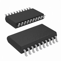
IC CTRLR PWM FULL-BRDG 20-QSOP
Manufacturer
Intersil
Datasheet
1.ISL6754AAZA-T.pdf
(19 pages)
Specifications of ISL6754AAZA
Pwm Type
Voltage/Current Mode
Number Of Outputs
6
Frequency - Max
2MHz
Duty Cycle
100%
Voltage - Supply
9 V ~ 16 V
Buck
No
Boost
No
Flyback
No
Inverting
No
Doubler
No
Divider
No
Cuk
No
Isolated
No
Operating Temperature
-40°C ~ 105°C
Package / Case
20-QSOP
Frequency-max
2MHz
Lead Free Status / RoHS Status
Lead free / RoHS Compliant
Available stocks
Company
Part Number
Manufacturer
Quantity
Price
Company:
Part Number:
ISL6754AAZA
Manufacturer:
Intersil
Quantity:
522
Company:
Part Number:
ISL6754AAZA-T
Manufacturer:
Intersil
Quantity:
1 900
maintains the current, which now circulates around the path
of switch UR, the transformer primary, and switch UL. When
switch LL opens, the output inductor current free-wheels
predominantly through diode D1. Diode D2 may actually
conduct very little or none of the free-wheeling current,
depending on circuit parasitics. This condition persists
through the remainder of the half-cycle.
When the upper switches toggle, the primary current that
was flowing through UR must find an alternate path. It
charges/discharges the parasitic capacitance of switches UR
and LR until the body diode of LR is forward biased. If
RESDEL is set properly, switch LR will be turned on at this
time.
The first power transfer period commences when switch LR
closes and the cycle repeats. The ZVS transition requires
that the leakage inductance has sufficient energy stored to
fully charge the parasitic capacitances. Since the energy
stored is proportional to the square of the current (1/2 L
the ZVS resonant transition is load dependent. If the leakage
inductance is not able to store sufficient energy for ZVS, a
discrete inductor may be added in series with the
transformer primary.
Synchronous Rectifier Outputs and Control
The ISL6754 provides double-ended PWM outputs, OUTLL
and OUTLR, and synchronous rectifier (SR) outputs,
OUTLLN and OUTLRN. The SR outputs are the
complements of the PWM outputs. It should be noted that
the complemented outputs are used in conjunction with the
VIN+
VIN+
VIN-
VIN-
FIGURE 19. UPPER SWITCH TOGGLE AND RESONANT
UL
LL
UL
LL
FIGURE 18. UR - UL FREE-WHEELING PERIOD
I
I
P
P
TRANSITION
UR
UR
LR
LR
L
L
L
L
17
D1
D2
D1
D2
I
I
S
S
L
I
VOUT+
VOUT+
P
RTN
RTN
2
),
ISL6754
opposite PWM output, i.e. OUTLL and OUTLRN are paired
together and OUTLR and OUTLLN are paired together.
Referring to Figure 20, the SRs alternate between being both
on during the free-wheeling portion of the cycle (OUTLL/LR
off), and one or the other being off when OUTLL or OUTLR is
on. If OUTLL is on, its corresponding SR must also be on,
indicating that OUTLRN is the correct SR control signal.
Likewise, if OUTLR is on, its corresponding SR must also be
on, indicating that OUTLLN is the correct SR control signal.
A useful feature of the ISL6754 is the ability to vary the
phase relationship between the PWM outputs (OUTLL, OUT
LR) and the their complements (OUTLLN, OUTLRN) by
±300ns. This feature allows the designer to compensate for
differences in the propagation times between the PWM FETs
and the SR FETs. A voltage applied to V
phase relationship.
FIGURE 21. WAVEFORM TIMING WITH PWM OUTPUTS
OUTLRN
OUTLRN
OUTLLN
OUTLLN
OUTLR
OUTLR
OUTLL
OUTLL
(SR1)
(SR2)
(SR1)
(SR2)
CT
CT
FIGURE 20. BASIC WAVEFORM TIMING
DELAYED, 0V < V
ADJ
< 2.425V
ADJ
controls the
September 29, 2008
FN6754.1


