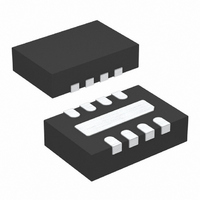
LTC3408EDD Linear Technology, LTC3408EDD Datasheet - Page 10

LTC3408EDD
Manufacturer Part Number
LTC3408EDD
Description
IC REG BUCK W/BYPASS TXRX 8-DFN
Manufacturer
Linear Technology
Datasheet
1.LTC3408EDD.pdf
(12 pages)
Specifications of LTC3408EDD
Applications
Converter, WCDMA Power Amplifier Applications
Voltage - Input
2.5 ~ 5 V
Number Of Outputs
1
Voltage - Output
0.3 ~ 3.5 V
Operating Temperature
-40°C ~ 85°C
Mounting Type
Surface Mount
Package / Case
8-DFN
Lead Free Status / RoHS Status
Contains lead / RoHS non-compliant
Available stocks
Company
Part Number
Manufacturer
Quantity
Price
Company:
Part Number:
LTC3408EDD
Manufacturer:
LINEAR
Quantity:
50
LTC3408
APPLICATIO S I FOR ATIO
I
charges of the internal top and bottom switches. Both the
DC bias and gate charge losses are proportional to V
thus, their effects will be more pronounced at higher
supply voltages. (The gate charge of the bypass FET is,
of course, negligible because it is infrequently cycled.)
2. I
internal switches, R
tinuous mode, the average output current flowing through
inductor L is “chopped” between the main switch and the
synchronous switch. Thus, the series resistance looking
into the SW pin is a function of both top and bottom
MOSFET R
The R
obtained from the Typical Performance Charateristics
curves. Hence, to obtain I
and multiply the result by the square of the average output
current.
Other losses including C
losses and inductor core losses generally account for less
than 2% total additional loss.
Thermal Considerations
In most applications the LTC3408 does not dissipate
much heat due to its high efficiency. But, in applications
where the LTC3408 is running at high ambient tempera-
ture with low supply voltage and high duty cycles, such as
in dropout, the heat dissipated may exceed the maximum
10
GATECHG
R
2
SW
R losses are calculated from the resistances of the
DS(ON)
= (R
0.01
0.01
= f(Q
0.1
DS(ON)
1
Figure 4. Power Lost vs Load Current
DS(ON)TOP
for both the top and bottom MOSFETs can be
1
T
+ Q
and the duty cycle (DC) as follows:
U
SW
LOAD CURRENT (mA)
B
)(DC) + (R
10
), where Q
, and external inductor R
2
U
R losses, simply add R
IN
and C
100
DS(ON)BOT
V
V
V
V
T
OUT
OUT
OUT
OUT
W
and Q
OUT
= 1.2V
= 1.5V
= 1.8V
= 2.5V
3408 F04
ESR dissipative
1000
B
)(1 – DC)
100
90
80
70
60
50
40
30
20
10
0
are the gate
U
L
. In con-
SW
to R
IN
L
,
junction temperature of the part. If the junction tempera-
ture reaches approximately 150°C, both power switches
will be turned off and the SW node will become high
impedance.
To prevent the LTC3408 from exceeding the maximum
junction temperature, the user will need to do some
thermal analysis. The goal of the thermal analysis is to
determine whether the power dissipated exceeds the
maximum junction temperature of the part. The tempera-
ture rise is given by:
where PD is the power dissipated by the regulator and θ
is the thermal resistance from the junction of the die to the
ambient temperature.
The junction temperature, T
where T
As an example, consider the LTC3408 in dropout at an
input voltage of 2.7V, a load current of 600mA (0.9V ≤ V
< 1.2V) and an ambient temperature of 70°C. With V
1.2V, the entire 600mA flows through the main P-channel
FET. From the typical performance graph of switch resis-
tance, the R
approximately 0.52Ω. Therefore, power dissipated by the
part is:
For the 8L DFN package, the θ
junction temperature of the regulator is:
which is below the maximum junction temperature of
125°C.
Modifying this example, suppose that V
1.2V or higher. This turns on the bypass P-channel FET as
well as the main P-channel FET. Assume that the inductor’s
DC resistance is 0.1Ω, the R
switch is 0.52Ω, and the R
switch is 0.08Ω. The current through the P-channel switch
and the inductor will be 69mA, causing power dissipation
of (0.069A)
T
T
PD = (I
T
R
J
J
= T
= 70°C + (0.1872)(43) = 78°C
= (PD)(θ
A
A
is the ambient temperature.
LOAD
+ T
2
DS(ON)
R
• 0.62Ω = 2.9mW. The bypass FET will
2
JA
) • R
)
of the P-channel switch at 70°C is
DS(ON)
DS(ON)
= 187.2mW
J
DS(ON)
, is given by:
JA
of the bypass P-channel
is 43°C/W. Thus, the
of the main P-channel
REF
is raised to
REF
3408f
REF
JA
<


