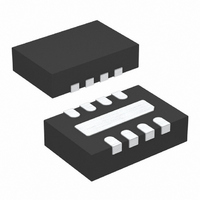
LTC3408EDD Linear Technology, LTC3408EDD Datasheet - Page 9

LTC3408EDD
Manufacturer Part Number
LTC3408EDD
Description
IC REG BUCK W/BYPASS TXRX 8-DFN
Manufacturer
Linear Technology
Datasheet
1.LTC3408EDD.pdf
(12 pages)
Specifications of LTC3408EDD
Applications
Converter, WCDMA Power Amplifier Applications
Voltage - Input
2.5 ~ 5 V
Number Of Outputs
1
Voltage - Output
0.3 ~ 3.5 V
Operating Temperature
-40°C ~ 85°C
Mounting Type
Surface Mount
Package / Case
8-DFN
Lead Free Status / RoHS Status
Contains lead / RoHS non-compliant
Available stocks
Company
Part Number
Manufacturer
Quantity
Price
Company:
Part Number:
LTC3408EDD
Manufacturer:
LINEAR
Quantity:
50
forced continuous mode, the LTC3408 will actually pull
current from the output until the command from V
satisfied. On alternate half cyles, this current actually exits
the V
forcing current into the battery. To prevent deterioration
of the battery, use sufficient bulk capacitance with low
ESR; at least 10µF is recommended.
Using Ceramic Input and Output Capacitors
Higher values, lower cost ceramic capacitors are now
becoming available in smaller case sizes. Their high ripple
current, high voltage rating and low ESR make them ideal
for switching regulator applications. Because the
LTC3408’s control loop does not depend on the output
capacitor’s ESR for stable operation, ceramic capacitors
can be used freely to achieve very low output ripple and
small circuit size.
However, care must be taken when ceramic capacitors are
used at the input and the output. When a ceramic capacitor
is used at the input and the power is supplied by a wall
adapter through long wires, a load step at the output can
induce ringing at the input, V
couple to the output and be mistaken as loop instability. At
worst, a sudden inrush of current through the long wires
can potentially cause a voltage spike at V
to damage the part.
When choosing the input and output ceramic capacitors,
choose the X5R or X7R dielectric formulations. These
dielectrics have the best temperature and voltage charac-
teristics of all the ceramics for a given value and size.
Ceramic capacitors of Y5V material are not recommended
because normal operating voltages cause their bulk ca-
pacitance to become much less than the nominal value.
Programming the Output Voltage With a DAC
The output voltage can be dynamically programmed to any
voltage from 0.3V to 3.5V with an external DAC driving the
REF pin. When the output is commanded low, the output
voltage descends quickly in forced continuous mode
pulling current from the output and transferring it to the
input. If the input is not connected to a low impedance
source capable of absorbing the energy, the input voltage
could rise above the absolute maximum voltage of the part
APPLICATIO S I FOR ATIO
IN
terminal, potentially causing a rise in V
U
U
IN
. At best, this ringing can
W
IN
large enough
U
IN
REF
and
is
and get damaged. The faster V
higher is the voltage spike at the input. For best results,
ramp the REF pin from high to low as slow as the
application will allow. Avoid abrupt changes in voltage of
>0.2V/µs. If ramp control is unavailable, an RC filter with
a time constant of 10µs can be inserted between the REF
pin and the DAC as shown in Figure 3.
Efficiency Considerations
The efficiency of a switching regulator is equal to the
output power divided by the input power times 100%. It is
often useful to analyze individual losses to determine what
is limiting the efficiency and which change would produce
the most improvement. Efficiency can be expressed as:
where L1, L2, etc. are the individual losses as a percentage
of input power.
Although all dissipative elements in the circuit produce
losses, two main sources usually account for most of the
losses in LTC3408 circuits: V
losses. The V
ciency loss at low load currents whereas the I
nates the efficiency loss at medium to high load currents.
In a typical efficiency plot, the efficiency curve at low load
currents can be misleading since the actual power lost is
of little consequence as illustrated in Figure 4.
1. The V
the DC bias current as given in the electrical characteris-
tics and the internal main switch and synchronous switch
gate charge currents. The gate charge current results
from switching the gate capacitance of the internal power
MOSFET switches. Each time the gate is switched from
high to low to high again, a packet of charge, dQ, moves
from V
than the DC bias current. In continuous mode,
Efficiency = 100% – (L1 + L2 + L3 + ...)
IN
IN
to ground. The resulting dQ/dt is typically larger
quiescent current consists of two components:
IN
DAC
Figure 3. Filtering the REF Pin
quiescent current loss dominates the effi-
10k
1000pF
IN
OUT
quiescent current and I
REF
is commanded low, the
LTC3408
GND
3408 F03
LTC3408
2
R loss domi-
9
3408f
2
R


