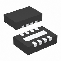
LTC3408EDD Linear Technology, LTC3408EDD Datasheet - Page 2

LTC3408EDD
Manufacturer Part Number
LTC3408EDD
Description
IC REG BUCK W/BYPASS TXRX 8-DFN
Manufacturer
Linear Technology
Datasheet
1.LTC3408EDD.pdf
(12 pages)
Specifications of LTC3408EDD
Applications
Converter, WCDMA Power Amplifier Applications
Voltage - Input
2.5 ~ 5 V
Number Of Outputs
1
Voltage - Output
0.3 ~ 3.5 V
Operating Temperature
-40°C ~ 85°C
Mounting Type
Surface Mount
Package / Case
8-DFN
Lead Free Status / RoHS Status
Contains lead / RoHS non-compliant
Available stocks
Company
Part Number
Manufacturer
Quantity
Price
Company:
Part Number:
LTC3408EDD
Manufacturer:
LINEAR
Quantity:
50
ABSOLUTE AXI U RATI GS
(Note 1)
Note 1: Absolute Maximum Ratings are those values beyond which the life
of a device may be impaired.
Note 2: The LTC3408E is guaranteed to meet performance specifications
from 0°C to 70°C. Specifications over the –40°C to 85°C operating
LTC3408
Input Supply Voltage (< 300µs) .................. – 0.3V to 6V
Input Supply Voltage (DC) ....................... – 0.3V to 5.5V
RUN, REF, V
SW Voltage (DC) ......................... – 0.3V to (V
P-Channel Switch Source Current (DC) ............. 800mA
N-Channel Switch Sink Current (DC) ................. 800mA
Peak SW Sink and Source Current ........................ 1.3A
Bypass P-Channel FET Source Current (DC) .............. 1A
Operating Temperature Range (Note 2) .. – 40°C to 85°C
Junction Temperature (Note 3) ............................ 125°C
Storage Temperature Range ................ – 65°C to 125°C
The
V
SYMBOL
V
∆V
I
V
V
I
f
V
R
R
R
I
I
V
I
I
ELECTRICAL CHARACTERISTICS
2
PK
S
OSC
LSW
LBYP
RUN
REF
OUT
LOADREG
IN
REF
RUN
IN
PFET
NFET
BYPASS
OUT
= 3.6V unless otherwise specified.
●
denotes specifications which apply over the full operating temperature range, otherwise specifications are T
PARAMETER
Regulated Output Voltage
Output Voltage Line Regulation
Peak Inductor Current
Output Voltage Load Regulation
Input Voltage Range
Input Current
Shutdown Current
Oscillator Frequency
Bypass PFET Turn-Off Threshold
Bypass PFET Turn-On Threshold
R
R
R
SW Leakage
Bypass PFET Leakage
RUN Threshold
RUN Input Current
REF Input Current
DS(ON)
DS(ON)
DS(ON)
OUT
Voltages .......................... – 0.3V to V
of P-Channel FET
of N-Channel FET
of Bypass P-Channel FET
W
W W
CONDITIONS
V
V
V
V
V
V
V
V
V
V
I
I
I
I
I
I
V
V
V
SW
SW
SW
SW
OUT
OUT
REF
REF
IN
IN
RUN
RUN
REF
REF
REF
REF
RUN
OUT
RUN
= 2.5V to 5V, V
= 3V, V
= 160mA, Wafer Level
= 160mA, DD Package
= –160mA, Wafer Level
= –160mA, DD Package
U
= 100mA, V
= 100mA, V
= 1.1V
= 0.1V
≥ 0.25V
≤ 0.1V
=
=
= 0V, V
= 1.2V, SW = Open
= 0V, SW = Open
= 0V, V
= 0V or 2.5V
IN
REF
+ 0.3V)
IN
SW
= 0.9V
= 5V, V
IN
IN
= 0V or 5V, V
IN
REF
= 3V, Wafer Level
= 3V, DD Package (Note 4)
REF
= 0.6V
PACKAGE/ORDER I FOR ATIO
= 0V
Consult LTC Marketing for parts specified with wider operating temperature ranges.
temperature range are assured by design, characterization and correlation
with statistical process controls.
Note 3: T
dissipation P
IN
LTC3408: T
T
8-LEAD (3mm × 3mm) PLASTIC DFN
JMAX
V
= 5V
GND
OUT
V
SW
EXPOSED PAD IS GND (PIN 9)
MUST BE SOLDERED TO PCB
IN
J
= 125°C, θ
is calculated from the ambient temperature T
1
2
3
4
D
according to the following formula:
DD PACKAGE
J
TOP VIEW
= T
JA
9
= 43°C/ W, θ
A
+ (P
D
)(43°C/W)
8
7
6
5
●
●
●
●
●
●
●
●
JC
V
V
REF
RUN
= 3°C/ W
OUT
IN
1.167
3.23
0.25
0.70
MIN
550
2.5
1.2
0.3
U
±0.01
±0.01
±0.01
±0.01
DD PART MARKING
1.21
0.05
0.08
TYP
700
3.3
0.3
0.1
1.5
0.1
1.5
1.2
0.3
0.4
0.3
0.4
0.7
1
1
ORDER PART
LTC3408EDD
A
NUMBER
W
= 25°C.
LAEA
A
MAX
3.37
0.35
1.25
1.26
0.08
850
0.4
2.5
1.8
0.4
0.4
1.5
±1
±1
±1
±1
and power
5
1
UNITS
U
MHz
3408f
%/V
kHz
mA
µA
µA
µA
µA
µA
%
Ω
Ω
Ω
Ω
Ω
Ω
V
V
A
V
V
V
V


