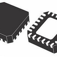
PM6641 STMicroelectronics, PM6641 Datasheet - Page 26

PM6641
Manufacturer Part Number
PM6641
Description
IC MONO VR DDR2/3 PC VFQFPN-48
Manufacturer
STMicroelectronics
Datasheet
1.PM6641TR.pdf
(47 pages)
Specifications of PM6641
Applications
Converter, DDR2, DDR3
Voltage - Input
2.7 ~ 5.5 V
Number Of Outputs
3
Voltage - Output
0.8 ~ 5.5 V
Operating Temperature
0°C ~ 85°C
Mounting Type
Surface Mount
Package / Case
48-VFQFN
Output Voltage
0.9 V
Output Current
3 A
Input Voltage
2.7 V to 5.5 V
Switching Frequency
1000 KHz
Operating Temperature Range
- 40 C to + 125 C
Mounting Style
SMD/SMT
For Use With
497-8425 - KIT EVAL PM6641 CHIPSET/DDR2/3
Lead Free Status / RoHS Status
Lead free / RoHS Compliant
Available stocks
Company
Part Number
Manufacturer
Quantity
Price
Company:
Part Number:
PM6641
Manufacturer:
BITECHNOL
Quantity:
2 000
Part Number:
PM6641
Manufacturer:
ST
Quantity:
20 000
Company:
Part Number:
PM6641TR
Manufacturer:
STM
Quantity:
35 839
Device description
7.4
26/47
SW regulators pulse skipping and PWM mode
In order to enhance the light load efficiency each switching regulator enters the pulse
skipping algorithm when the output current sourced is too low. The threshold load current
which allows the regulator to enter the pulse skipping mode can be estimated with the
following formula: (Vi-Vo)/(2Lfsw)*Vo/Vi
Equation 4
When the load current is lower than I
cycle, decreasing the effective switching frequency and, as a consequence, reducing the
switching losses. This mode of operation is guaranteed by the presence of the zero crossing
current comparator, the internal block which senses the inductor current and avoids this
current to becoming negative, in the normal operating condition.
The inductor current is allowed to become negative when the output voltage rises above the
+10% power good threshold. In this condition of output soft over voltage the zero crossing
current comparator is deactivated and the pulse skipping algorithm is replaced by the typical
PWM one; as a consequence each switching regulator can sink up to some hundreds milli
amps to decrease the output voltage to the nominal value.
Figure 29. SW regulators pulse skipping and PWM mode
a) Pulse Skipping Mode
a) Pulse Skipping Mode
Doc ID 13510 Rev 3
Iomin
Clock
Clock
Omin
Vout
Vout
I
I
L
L
value, the switching regulator begins to skip some
≈
(
----------------------- -
(
V
2Lf
I
–
SW
V
O
)
)
⋅
V
-------
V
O
I
b) PWM Mode
b) PWM Mode
Clock
Clock
Vout
Vout
I
I
L
L
PM6641


