PM6641 STMicroelectronics, PM6641 Datasheet - Page 30

PM6641
Manufacturer Part Number
PM6641
Description
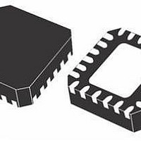
IC MONO VR DDR2/3 PC VFQFPN-48
Manufacturer
STMicroelectronics
Datasheet
1.PM6641TR.pdf
(47 pages)
Specifications of PM6641
Applications
Converter, DDR2, DDR3
Voltage - Input
2.7 ~ 5.5 V
Number Of Outputs
3
Voltage - Output
0.8 ~ 5.5 V
Operating Temperature
0°C ~ 85°C
Mounting Type
Surface Mount
Package / Case
48-VFQFN
Output Voltage
0.9 V
Output Current
3 A
Input Voltage
2.7 V to 5.5 V
Switching Frequency
1000 KHz
Operating Temperature Range
- 40 C to + 125 C
Mounting Style
SMD/SMT
For Use With
497-8425 - KIT EVAL PM6641 CHIPSET/DDR2/3
Lead Free Status / RoHS Status
Lead free / RoHS Compliant
Available stocks
Company
Part Number
Manufacturer
Quantity
Price
Company:
Part Number:
PM6641
Manufacturer:
BITECHNOL
Quantity:
2 000
Part Number:
PM6641
Manufacturer:
ST
Quantity:
20 000
Company:
Part Number:
PM6641TR
Manufacturer:
STM
Quantity:
35 839
Device description
7.9
30/47
Phase management
When all the three switching regulators high side MOSFETs are turned on simultaneously
the input root mean square (RMS) current could rise up to very high values, increasing the
system losses and inducing external components overheating. It’s possible to reduce the
input overall RMS current by inserting one ceramic capacitor as close as possible to each
switching regulator power supply input, reducing the impulsive input current path. However
this synchronous mode of operation is jitter-free and noise immune.
Another possible way to reduce the input RMS current is based on the phase shifting
technique, which decreases the total input current by delaying the regulators turn on pulse.
With three regulators turned on, the 120d e.g. phase shifting allows to reduce the overall
input current up to 1.73 times as depicted in the following configuration, in which three
independent regulators with Vout/Vin lower than 0.333 and identical output current (I) are
managed with synchronous or 120 deg phase shifted turning on.
Figure 32. SW regulator phase management
Each regulator RMS input current is easily computed:
Equation 7
defining T
SW
the switching period, equal to
I
I
I
Synchronous
I
L
L1
L2
L3
I
1
CIN
L ,
2
L ,
3
Doc ID 13510 Rev 3
+
+
=
=
T
SW
1
T
∫
SW
I
L
2
1
1
L ,
2
f
L ,
SW
3
dt
and T
=
120deg delay
I
I
L1
CIN
T
ON
+
+
=
SW
1
I
the high side MOSFET on time.
I
L2
2
T
ON
I
L3
PM6641


